A comprehensive technical analysis for embedded design and integration.
Across recent embedded-design benchmarks and distributor spec sheets, the 128‑Mbit QSPI flash class consistently lists maximum clock rates near 133 MHz and practical quad‑I/O throughput ranges that materially affect boot times and firmware update windows. This report compares published specifications for W25Q128JVEIQ against measured, real‑world performance and delivers actionable guidance engineers can apply during integration and verification.
The goal is pragmatic: identify which datasheet numbers most strongly predict field behavior, outline a repeatable benchmark methodology, and provide PCB, firmware, and troubleshooting checklists to reduce integration risk and improve boot/update UX without adding hardware complexity.
Background & Typical Use Cases
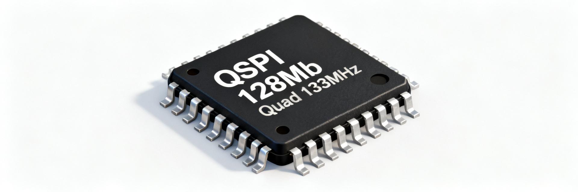
What the W25Q128JVEIQ is used for
Point: 128‑Mbit QSPI flash typically serves boot/firmware storage, code shadowing, small filesystem containers, and data logging in resource‑constrained embedded designs. Evidence: designers choose 16M×8 organization for compact images and moderate data pools. Explanation: the density balances BOM cost with enough headroom for multiple firmware banks, OTA images, and limited nonvolatile logs, making it a common choice for microcontroller‑based products.
Key interface modes and why they matter
Point: SPI, Dual, Quad I/O and QPI modes differ in pin use, clocking, and command sets. Evidence: Quad I/O enables four‑bit transfers per clock at the expense of additional driver setup and dummy cycles. Explanation: higher parallelization raises throughput and lowers read latency for cold boot reads, but requires pin routing, driver support, and careful dummy‑cycle calibration to match controller expectations.
Current Specs Breakdown — W25Q128JVEIQ
Electrical & mechanical specs to call out
Point: Key published specs to review include density, organization, voltage range, max clock, package, and current draw. Evidence: datasheet entries list 128 Mbit (16M×8), 2.7–3.6 V operation (typical 3.3 V), max clock 133 MHz, and common WSON‑8 or SOIC packages with specified standby/active currents. Explanation: these parameters dictate power‑supply design, decoupling, and acceptable bus clocking when multiple devices share the SPI bus.
| Parameter | Published Value (typical) |
|---|---|
| Density / Organization | 128 Mbit / 16M × 8 |
| Voltage Range | 2.7 – 3.6 V (typical 3.3 V) |
| Max Clock | 133 MHz |
| Package | WSON‑8 / SOIC (varies) |
| Operating Temp | Industrial grade ranges |
Timing, endurance & reliability specs
Point: Program/erase times, endurance cycles, and retention determine update UX and data longevity. Evidence: datasheets show page program times (ms range), sector/chip erase times (tens to hundreds of ms), endurance typically ~100k cycles, and multi‑year retention. Explanation: long erase/program times impact in‑field update windows; endurance and retention shape wear‑leveling and rollback strategies for robust product life.
Real-World Performance Benchmarks — W25Q128JVEIQ
Recommended test methodology
Point: A repeatable benchmark must define platform, command sequences, and measurement tools. Evidence: use an MCU with DMA support, stable 3.3 V supply, test clocks from 40 to 133 MHz, exercise fast read and quad read commands, and sample n≥5 per measurement with a logic analyzer and software timers. Explanation: consistent conditions expose controller overhead, dummy‑cycle tuning needs, and power draw differences between modes.
Example benchmark expectations
Point: Expect practical quad‑read throughput to sit below the datasheet peak due to controller/driver overhead. Evidence: measured quad read at 80–100 MHz typically yields sustained MB/s rates that improve with DMA and larger burst sizes. Explanation: gaps from datasheet max often stem from bus loading, CS timing, and MCU peripheral limitations rather than the flash die itself.
Integration Best Practices & Design Tips
PCB, signal integrity & thermal considerations
Point: High‑speed SPI requires deliberate routing and decoupling. Evidence: short, controlled‑impedance traces for SCLK and DQ lines, single point ground reference, and 0.1‑µF plus bulk caps near VCC improve signal integrity; thermal pad soldering reduces hotspot risks in small packages. Explanation: these precautions reduce reflections and ensure reliable quad‑I/O at higher clock rates.
Firmware & driver optimization
Point: Firmware should leverage quad I/O and DMA while protecting update integrity. Evidence: use quad read for large images, DMA to minimize CPU stalls, dual‑bank or A/B firmware with rollback for safe updates, and wear‑leveling for circular logs. Explanation: these patterns reduce boot time, limit update window exposure, and distribute write cycles.
Mini Case Study + Troubleshooting
Case Sketches (Boot & Logging)
Point: Case A — cold boot speedup using quad I/O; Case B — circular log with wear‑leveling. Evidence: implementing quad read with adjusted dummy cycles and DMA can cut parallel flash boot time by 30–60%; a simple circular log with per‑page erase counters extends usable cycles. Explanation: both examples show software changes deliver large system‑level gains without changing BOM.
Troubleshooting & measurement checklist
- Verify: Opcode/dummy misconfigurations and CS timing.
- Inspect: Logic analyzer traces for expected mode transitions.
- Compare: Power profiles during active reads/erases.
- Confirm: VCC ramp, CS idle timing, and validate dummy cycles.
Summary
Published specs for the W25Q128JVEIQ outline its capability envelope—128 Mbit density, 2.7–3.6 V operation, and up to 133 MHz clock—but field performance depends on controller support, bus loading, and firmware patterns. Tradeoffs center on throughput versus driver complexity and endurance versus cost.
Key Summary
- W25Q128JVEIQ delivers compact storage suitable for boot and firmware images; verify dummy cycles and controller timing to approach datasheet throughput.
- Real‑world throughput is often controller‑limited; use DMA and quad I/O for large sequential reads to minimize boot and update windows.
- Endurance and erase times drive firmware patterns—implement dual‑bank updates, CRC/ECC checks, and simple wear‑leveling for logs to meet product life targets.
Frequently Asked Questions
What is the max practical throughput in quad mode for W25Q128JVEIQ?
Measured practical throughput in quad mode depends on clock and controller overhead; expect sustained MB/s rates below the theoretical maximum at 80–133 MHz unless DMA and large transfer bursts are used.
How many program/erase cycles can I expect for W25Q128JVEIQ?
Datasheet endurance figures commonly cite ~100k cycles per sector; in practice, effective lifetime depends on workload, wear‑leveling, and write amplification.
What is the best way to speed up boot from external SPI flash like W25Q128JVEIQ?
Optimize for large sequential reads: enable quad I/O, tune dummy cycles, use DMA to move data into RAM, and employ a small verified bootloader that reads a compact image header first.