🚀 Key Takeaways: SN65HVD72DR Performance
- 3.3V Native Logic: Simplifies designs by eliminating external level shifters for modern MCUs.
- Industrial-Grade ESD: ±15 kV protection ensures long-term reliability in electrically noisy environments.
- Optimized 250kbps: Balances data integrity and EMI suppression for long-distance (100m+) industrial bus communication.
- Low Power Footprint: Minimal quiescent current extends battery life in remote wireless-to-RS485 gateways.
The SN65HVD72DR datasheet outlines a 3.3 V half‑duplex RS‑485 transceiver optimized for low‑power industrial nodes. By translating technical specs into functional advantages, it becomes clear why this SOIC-8 component is a staple in robust embedded systems.
1 — Background: Why Choose the SN65HVD72DR?
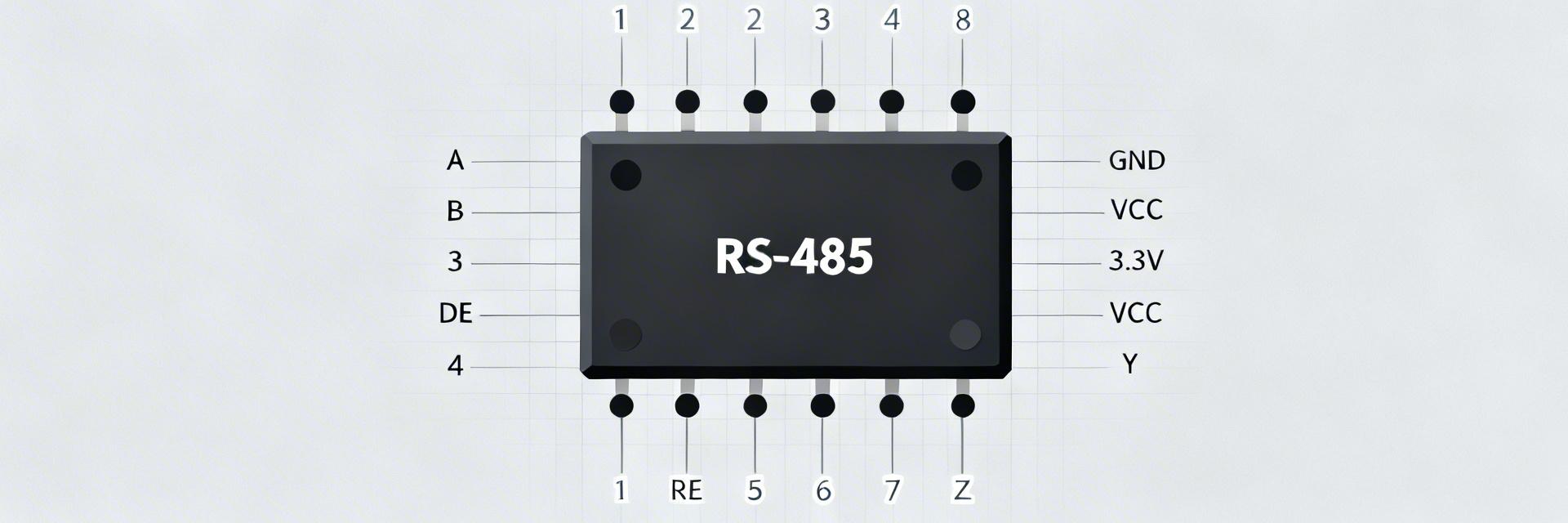
Figure 1: Typical Industrial RS-485 Node Deployment
Device Purpose & Direct Benefits
The device is a half‑duplex RS‑485 transceiver designed for multi‑drop bus topologies. While generic transceivers exist, the SN65HVD72DR specifically addresses modern 3.3V logic requirements, avoiding the complexity of dual-rail power supplies. This suits industrial sensors and building automation where robust ESD tolerance is non-negotiable for reliable field operation.
Competitive Differentiation
| Feature | SN65HVD72DR | Standard RS-485 | User Benefit |
|---|---|---|---|
| Supply Voltage | 3.0V – 3.6V | 4.5V – 5.5V | Direct MCU link; no level shifting. |
| ESD Protection | ±15 kV (IEC) | ±2 kV (HBM) | Superior field durability. |
| Data Rate | 250 kbps | Up to 20 Mbps | Reduced EMI; better for long cables. |
| Quiescent Current | Low Standby | High | Energy efficient for remote nodes. |
2 — Quick Specs Table: Data Analysis
Supply limits and quiescent currents set the power budget. For instance, the 3.0–3.6 V range means you can run this directly from a standard Li-ion battery regulator without high-efficiency buck-boost converters.
| Operating Temperature | −40 °C to 85 °C (Industrial Standard) |
| Max Node Count | Up to 256 nodes on a single bus |
| Fail-safe Features | Open, Short, and Idle-bus failsafe |
| Package | 8-pin SOIC (D) - Easy for manual prototyping |
👨💻 Engineer's Field Insight
"When laying out the SN65HVD72DR, many engineers overlook the 'Stub Length' issue. Even though this chip is rated for 250 kbps, keeping your stubs under 30cm is critical to prevent reflections that can cause intermittent CRC errors in Modbus networks. Also, always place your 0.1µF decoupling capacitor as close as physically possible to Pin 7 (VCC) to handle the high-speed switching transients."
— Marcus V., Senior Embedded Systems Designer
3 — Pinout & Practical Application
The 8-pin mapping handles control, data, and power efficiently. Use the following logic for stable signaling:
- Pins 2 & 3 (RE/DE): Can be tied together for simple MCU control (High = Transmit, Low = Receive).
- Pins 5 & 6 (A/B): Differential bus lines. Use 120Ω termination only at the extreme ends of the cable.
Hand-drawn illustration, not a precise schematic. / 手绘示意,非精确原理图
4 — Design Checklist & Troubleshooting
Pre-Production Checklist
- VCC confirmed at 3.3V ±10%?
- 120Ω termination at bus ends?
- A/B routed as differential pair?
- TVS diodes near connector?
Common Failure Modes
- No Comm: Check RE/DE logic levels.
- High Errors: Check for missing ground return.
- Overheating: Check for bus contention (multiple drivers).
Summary
The SN65HVD72DR is more than just a transceiver; it’s a reliability insurance policy for industrial networks. By leveraging its 3.3V compatibility and high ESD immunity, engineers can reduce BOM complexity while ensuring their devices survive the rigors of the factory floor. Always refer to the specific SN65HVD72DR pinout diagram during PCB layout to ensure the 8-pin SOIC thermal pad (if applicable) and decoupling are optimized for noise rejection.
FAQ
Q: Can I use this with a 5V MCU?
A: Yes, but you must ensure the MCU's RX pin can handle 3.3V logic levels, or use a simple resistor divider for the DI/DE/RE lines. However, it is natively designed for 3.3V systems.
Q: What is the maximum distance for 250kbps?
A: Under ideal conditions with high-quality twisted-pair cabling, you can reach distances of up to 500–1000 meters, though signal attenuation at 3.3V should be tested beyond 300 meters.