
The 74LS244 datasheet describes an octal TTL 3‑state buffer commonly used on 5 V digital buses — 20‑pin packages, two enable lines that gate two four‑bit sections, and datasheet DC/AC tables that define VIH/VIL, IOL/IOH and propagation delays. This article explains what to extract from the datasheet and how those anchors guide bench validation and system integration for dependable bus buffering and address/data isolation.
1 — What the 74LS244 Is and How to Read Its Datasheet (Background)
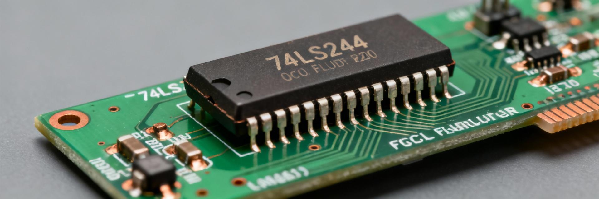
Functional overview
Point: The device is an octal buffer/line driver with 3‑STATE outputs used for bus driving and isolation. Evidence: Datasheet description frames it as two independent groups of four buffers with common enables. Explanation: That topology allows one chip to control two bus segments independently, simplifying address latch designs and reducing bus contention when enable sequencing is correct; LS TTL tradeoffs include limited fanout and a strict 5 V VCC requirement.
Package types and mechanical info
Point: Common form factors are 20‑pin DIP and 20‑pin SOIC; mechanical notes matter for layout. Evidence: The package section lists pin spacing, lead dimensions and recommended land patterns. Explanation: For reliable boards, use the datasheet land pattern and note the thermal pad/leads for solder fillets; 20‑pin spacing dictates routing density and minimal trace stubs to preserve signal integrity in TTL‑speed buses.
2 — Pinout & Functional Behavior (Pinout)
Pin mapping and signal names (authorable checklist)
Point: The canonical pin map places VCC and GND at standard pins and groups enables and octal I/O. Evidence: Datasheet pin tables show VCC, GND, 1G/2G (enables), A0–A7 (inputs) and Y0–Y7 (outputs). Explanation: Label diagrams to show which enable controls which quartet (typically A0–A3 ↔ Y0–Y3 and A4–A7 ↔ Y4–Y7) and mark enable polarity so silkscreen and schematic match the active‑state behavior on the bench.
Truth table and enable/3‑STATE behavior
Point: Enables place outputs into active drive or high‑impedance 3‑STATE. Evidence: The truth table in the datasheet enumerates enable = active → outputs follow inputs; enable = inactive → outputs high‑Z. Explanation: In practice, ensure unused outputs are not floating on a shared bus—tri‑stating enables for bus sharing requires defined enable sequencing and pull resistors or controlled master arbitration to prevent contention.
3 — Electrical Specs Deep Dive (Electrical Specs)
DC characteristics: how to read and apply them
Point: Key DC specs to extract are VCC operating range, VIH/VIL thresholds, IOH/IOL drive limits, ICC, and input/output leakage. Evidence: Datasheet DC tables separate guaranteed min/max from typical values and list absolute maximum ratings. Explanation: Use guaranteed limits for margins (e.g., assume VIH worst‑case when designing logic thresholds), spec IO margins per fanout and add guard bands for temperature — choose pull resistor values and power‑rail decoupling based on worst‑case ICC and I/O currents.
AC characteristics and load assumptions
Point: Timing numbers depend on test load and conditions; propagation delay and rise/fall times are not absolute constants. Evidence: AC tables specify conditions (VCC, CL, temperature) and list tPLH/tPHL, contamination delay and transition times. Explanation: Translate those into timing budgets by adding margin for worse CL and temperature; account for added trace capacitance and multiple loads when converting datasheet delays into setup/hold budgets in a real system.
4 — Bench Test Plan & Representative Measurements (Case / Data)
Recommended test setup and measurement methodology
Point: Reproducible tests require a controlled PCB, proper probes and defined loads. Evidence: Practical setups use a short‑trace test jig, regulated 5 V supply with decoupling, oscilloscope with 10X probe and logic analyzer for capture. Explanation: Measure propagation delay with matched coax/probe grounding to avoid artifact; use defined resistive loads or active TTL loads and document VCC, CL and temperature so measurements map back to datasheet conditions.
What results to expect and how to report them
Point: Reported categories should include tPD ranges, IO drive behavior, ICC under static and dynamic conditions and tri‑state verification. Evidence: Datasheet typicals give a baseline; real measurements often show wider spreads depending on manufacturer and lot. Explanation: Present annotated scope captures, a table of worst‑case vs typical values, and call out any deviations from datasheet limits along with test conditions so readers can judge margin and reproducibility.
| Parameter | Representative Datasheet Notes | Test Condition to Record |
|---|---|---|
| VCC operating range | Nominal 5 V ± tolerance | Exact VCC, ripple |
| VIH / VIL | TTL thresholds (VIH ≈ 2.0 V, VIL ≈ 0.8 V) | Measurement method, input source impedance |
| IOH / IOL | Output drive limits per output | Load resistor or active load |
| Propagation delay | Typical range listed; depends on CL | CL value, scope probe loading |
Quick visual (for numeric anchors listed)
5 — Design Integration & Troubleshooting Checklist (Actionable Advice)
Integration best practices
Point: Follow layout and system rules to avoid common pitfalls. Evidence: Datasheet layout notes and recommended decoupling placements indicate best practices. Explanation: Place 0.1 µF decouplers close to VCC pin, tie unused inputs to defined levels with pull resistors, sequence enables to prevent transient contention, and consider series resistors or level translators when interfacing to non‑TTL domains.
Common failure modes and debugging tips
Point: Typical failure modes are bus contention, floating inputs and excessive ICC. Evidence: Symptoms such as overheating, slow edges or logic glitches correlate to datasheet limits being exceeded. Explanation: Use a stepwise isolation approach — disable sections, verify enables, measure ICC, clamp outputs with known loads, and add series resistors or adjust enable timing to eliminate contention and restore expected behavior.
Summary
This guide showed how to extract the critical anchors from the 74LS244 datasheet and translate them into bench tests and design rules so the octal TTL buffer can be validated and integrated reliably. Key actions are to document DC/AC test conditions, follow package and layout notes, run the recommended propagation and drive tests, and verify tri‑state behavior before system deployment.
Key Summary
- Extract pinout and enable polarity early so schematic silkscreen and PCB labeling match the datasheet and prevent incorrect wiring during testing.
- Use guaranteed DC limits (VIH/VIL, IOH/IOL, ICC) for margins; typical values are informative but not safe for worst‑case design decisions.
- Measure propagation delay and output drive with documented CL, probe setup and VCC; present worst‑case numbers and annotated scope captures for reproducibility.
Common Questions and Answers
How do I test 74LS244 outputs for propagation delay?
Measure from a clean input edge to the corresponding output edge with a low‑capacitance probe, record the load capacitance (CL) and VCC, and repeat for rising and falling transitions; report tPLH/tPHL alongside CL to map results against datasheet timing tables.
What pinout should I follow for 74LS244 pin mapping?
Use the datasheet pin table: VCC and GND on the power pins, two enables controlling two groups of four buffers, A0–A7 as inputs and Y0–Y7 as outputs; label PCB silkscreen to show enable polarity and group boundaries to avoid wiring mistakes.
Which electrical specs matter most when designing with a 74LS244?
Prioritize VCC tolerance, VIH/VIL thresholds, IOH/IOL drive limits and ICC for power budgeting; those determine reliable logic recognition, fanout, and thermal/power behavior — always design with the datasheet’s guaranteed limits rather than typical values.








