
74LS20 datasheet: Compact Specs & Test Data Summary
The 74LS20 datasheet condenses the electrical and timing parameters that matter for designers working with 5 V TTL logic. This concise reference pulls together the essential published specs and practical bench test guidance so an engineer can quickly validate timing, drive and power in legacy systems. The introduction focuses on the parameters most relevant to real‑world timing and power budgets.
Engineers familiar with TTL LS families will recognize the recurring spec categories—propagation delay, input/output thresholds, ICC and fan‑out—that govern system behavior. The following sections summarize device identity, compact specs tables, variability analysis, bench test procedures, example circuits and a practical checklist for rapid integration and verification.
Background: What the 74LS20 is and where it fits
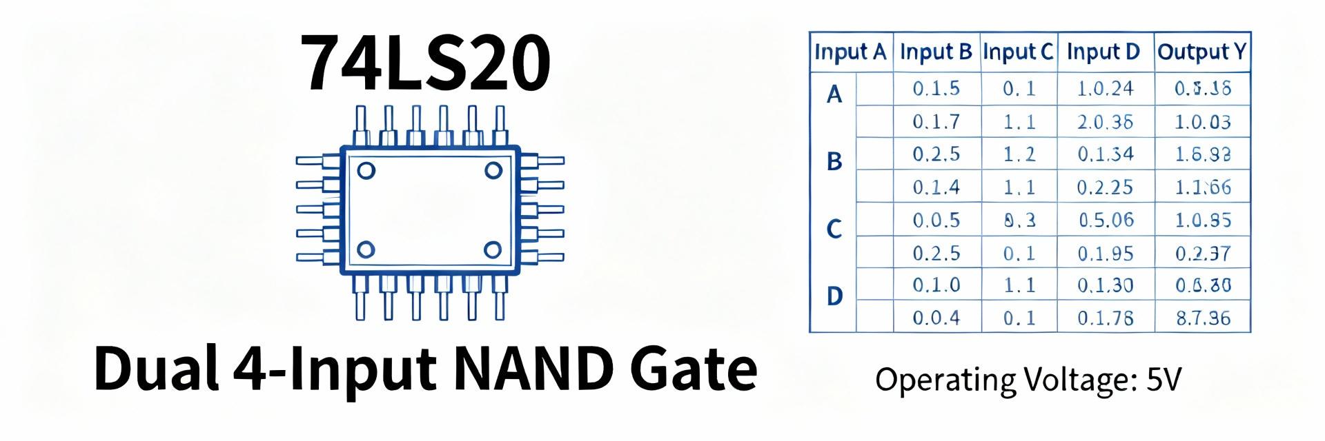
Key device identity
The device is a dual 4‑input positive‑NAND in the TTL LS family, providing two independent gates each combining four inputs into a NAND output. Typical package options include 14‑pin DIP and 14‑pin SOIC for through‑hole and surface‑mount use. The short functional description, pinout and absolute ratings are the first things to capture when consulting the device specs.
Typical use cases and legacy relevance
Common applications include glue logic, bus control gating, interrupt enables and simple combinational functions where four‑input NAND reduces IC count. Designers still consult the 74LS20 datasheet because of long availability, well‑documented behavior under standard TTL loads and predictable timing that eases retrofit work in mixed‑logic systems.
Compact Specs: Electrical characteristics at a glance
Recommended table: core electrical specs (must include)
This section condenses the core specs designers copy from the datasheet: VCC, input thresholds (VIH/VIL), output levels (VOH/VOL), ICC quiescent current, IOH/IOL output drive, fan‑out and power dissipation. Present values under standard conditions (VCC = 5 V, TA = 25°C) and annotate any test load assumptions so the numbers map directly to design margins.
| Parameter | Test Condition | Typical / Max |
|---|---|---|
| VCC | - | 5 V nominal |
| VIH | VCC = 5 V | 2.0 V (min) |
| VIL | VCC = 5 V | 0.8 V (max) |
| VOH | IOH = -0.4 mA | 2.4 V (min) |
| VOL | IOL = 8 mA | 0.5 V (max) |
| ICC | All inputs high | Typically a few mA, see datasheet max |
| IOH / IOL | Standard TTL test loads | See output drive specs |
| Fan‑out | - | Standard TTL fan‑out (≤10) |
| Power dissipation | Per package | See datasheet thermal limits |
Timing & dynamic parameters
Key dynamic numbers are propagation delays (tPLH/tPHL), contamination delay, and rise/fall times. Datasheets list typical and guaranteed maximum propagation delays per gate under specified loads; designers should read the timing footnotes to understand test loads and definitions. A compact timing diagram showing input edge to output transition clarifies how to extract tPLH/tPHL values from the tables.
Data analysis: Comparing published values & common tolerances
Variability across datasheets and part batches
Propagation delay and supply current can vary by vendor revision and lot. Typical reported propagation delays for LS devices fall into a range with a guaranteed maximum; ICC is often given as a typical value with a higher guaranteed max. Temperature and heavier loading increase delay and current; always consult datasheet footnotes to reconcile differing tables.
What spec variations mean for system design
Translate specs to design margins: use the datasheet maximum propagation delay plus a safety margin when budgeting timing. A practical rule is to use the datasheet max propagation delay plus 20% margin per gate cascade to cover temperature and loading effects. For power budgeting, plan for datasheet max ICC and account for dynamic switching currents under expected toggle rates.
Test data: How to verify 74LS20 behavior on the bench
Recommended test setup and conditions
Bench verification requires an oscilloscope or high‑speed logic analyzer, clean TTL‑level input drivers, a stable 5 V supply with local bypass (0.1 µF), and standard TTL load resistors for output measurement. Probe outputs under the datasheet test load conditions to measure VOH/VOL. Measure ICC with a low‑noise power supply and record ambient temperature and load conditions for traceability.
Standard test procedures and expected data presentation
Measure propagation delay by driving an input with a fast edge, probing input and output with the same oscilloscope ground reference and recording tPLH/tPHL. For output drive, measure VOH/VOL at the datasheet IOH/IOL points. Record results in a concise table: parameter, datasheet typ/max, bench measured, test conditions, pass/fail. Note deviations and likely causes such as temperature, loading, or aged parts.
Typical circuits & example use cases
Example reference circuits
Example 1: single 4‑input NAND used as an enable—expect a single gate propagation delay. Example 2: cascaded NANDs for expanded input functions—accumulate gate delays per stage. In both cases include a 0.1 µF bypass capacitor at VCC near the package and keep trace lengths short to minimize ringing and timing uncertainty.
Troubleshooting checklist for circuit behavior
When outputs are stuck or timing fails, check: VCC presence and bypassing, input levels vs thresholds, excessive output loading, and temperature. Cross‑check measured VOH/VOL and ICC against datasheet specs and bench test data. Replace suspect ICs and compare measured parameters to expected ranges to identify counterfeit or degraded parts.
Practical action checklist & quick reference
What to copy from the datasheet into your design doc
Copy these items verbatim into a design reference: VCC and recommended supply decoupling, VIH/VIL thresholds, VOH/VOL with IO conditions, IOH/IOL drive specs, propagation delays (tPLH/tPHL), ICC quiescent and max, absolute maximum ratings and thermal limits, and the package pinout used in your design. Note the exact datasheet revision used for traceability.
SEO & download tips (writer-actionable)
Suggested long‑tail titles for documentation include example taglines such as "74LS20 datasheet summary: pinout, specs & test data" and "How to test 74LS20 propagation delay." Offer a one‑page downloadable CSV or PDF that lists measured test data alongside datasheet values to aid verification and on‑site troubleshooting.
Summary
The 74LS20 datasheet quick reference provides the essential specs and practical test data engineers need to validate timing, drive and power in 5 V TTL systems. A compact spec table, comparable timing numbers, a standard bench procedure and a troubleshooting checklist enable a rapid path from documentation to verified implementation.
- Include VCC, VIH/VIL thresholds and VOH/VOL with IO conditions from the datasheet so the design meets input/output tolerance requirements and aligns with measured test data.
- Record propagation delays (tPLH/tPHL) and use datasheet max plus 20% margin per cascade to budget worst‑case timing and avoid race conditions.
- Test ICC and output drive under the datasheet test loads and document measured values in a CSV to compare against specs and track part variability.
Frequently Asked Questions
How should propagation delay be measured on the bench?
Use a single‑channel pulse generator to drive the input, probe the input and the corresponding output with an oscilloscope using the same ground reference, and measure the time difference between the 50% transition points for tPLH and tPHL. Record the test load and ambient temperature alongside the measurement for reproducibility.
Which load values are appropriate for VOH/VOL verification?
Use the standard TTL test loads specified in the device documentation—typically a light pull‑up for VOH and a defined sinking current for VOL. Measure voltage at the output under those IOH/IOL conditions and compare to the datasheet guaranteed levels; note that heavier loads will raise VOL and lower VOH.
What are common causes for discrepancies between datasheet and measured results?
Common causes include incorrect test loads, insufficient bypassing, temperature extremes, aged or counterfeit ICs, and measurement setup errors such as ground bounce or probe capacitance. Verify test conditions match the datasheet and repeat tests while isolating variables to pinpoint the root cause.








