
Measured against common medium‑power PNP devices, the BCX53-16 stands out with its 80 V collector-emitter rating and 1 A collector current—key numbers that determine suitability for AF drivers, small power stages and general switching tasks. This report gives a concise datasheet-level snapshot, lab benchmarks to expect, and practical integration guidance so designers can decide quickly whether the part meets their thermal, gain and saturation needs.
The focus is concise and data-driven: highlight the electrical and thermal limits, outline bench tests with sample expectations, and provide PCB and biasing rules that reduce rework risk in prototyping and small-volume production. Where measurement tolerances matter, test conditions are specified so results map directly to design margins and verification steps for pre-production sign-off.
Background: What the BCX53-16 Is and Where It Fits
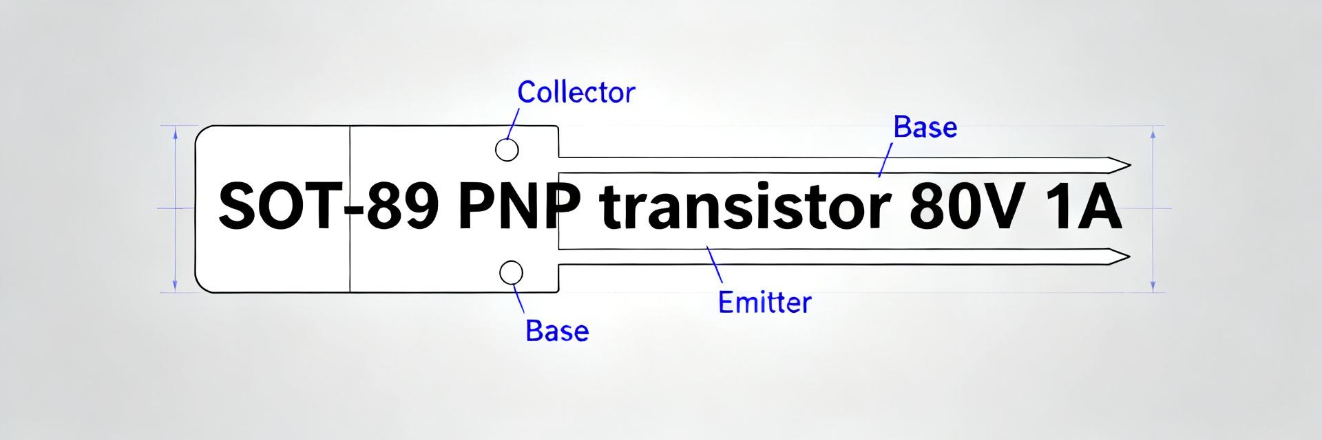
Device overview & package
Point: This family positions as a medium‑power PNP BJT in a compact SOT‑89 flat‑lead surface‑mount package suited to constrained PCBs. Evidence: Datasheet headline numbers place the device at roughly an 80 V Vce rating and a 1 A continuous collector current with package-dependent power dissipation limits. Explanation: The SOT‑89 form factor balances thermal mass and footprint; expect Pd specifications that assume limited PCB copper and require derating at elevated ambient temperatures for continuous loads.
Typical applications
Point: Typical uses include audio (AF) driver stages, small motor drivers, level shifting and general switching in medium‑voltage circuits. Evidence: The voltage and current envelope plus moderate gain make the device practical for complementary amplifier legs or as a high‑side driver when matched to the circuit’s SOA. Explanation: Because SOT‑89 imposes thermal limits, designers should prefer this PNP transistor for intermittent or low‑dissipation roles rather than high continuous power conversion where larger packages or MOSFETs are superior.
Key Specs at a Glance (Datasheet‑level)
Electrical ratings & DC parameters
Point: Key electrical specs to report are VCEO, IC (DC), VCE(sat) at defined Ib/Ic, DC current gain range (hFE) vs. Ic, leakage currents and fT. Evidence: For lab reporting, state absolute max VCE (~80 V), Ic capability (~1 A), typical VCE(sat) at specified Ib/Ic, hFE bands at low and moderate currents, and leakage growth with temperature. Explanation: Always annotate test conditions (Ta vs. Tj) and list typical versus guaranteed max values to avoid misreading datasheet “typical” figures as guaranteed performance.
| Parameter | Test condition | Typical | Max / Notes |
|---|---|---|---|
| VCEO | IC small-signal | — | ≈80 V |
| IC (DC) | VCE within SOA | — | 1 A |
| VCE(sat) | Ic=150 mA, Ib=15 mA | ~200–400 mV | Depends on Ib ratio |
| hFE | Ic range 1 mA–500 mA | ~50–200 | Falls at higher Ic |
| fT | Ic specified | — | Low-to-moderate (MHz class) |
Thermal, mechanical & package limits
Point: Thermal behavior is dominated by SOT‑89 RthJA, Pd at Tamb=25°C, and copper area on the PCB. Evidence: Typical SOT‑89 thermal resistance can range widely; datasheets tie Pd to a defined copper land area and often require derating per °C above 25°C. Explanation: Designers should assume a conservatively derated Pd for continuous operation (e.g., reduce rated Pd by 40–60% for cramped layouts or elevated ambient) and provide a minimum copper pad and short power traces to improve heat spreading.
Benchmarks & Comparative Performance (Data‑driven)
Typical bench tests and expected results
Point: Recommended bench tests are VCE(sat) vs. Ic at defined base drive, hFE vs. Ic, leakage vs. temperature, and basic switching timing where applicable. Evidence: In practice, expect VCE(sat) on the order of a few hundred millivolts at modest currents with base drive ratios ~1:10; hFE will peak at low-to-moderate currents and decline near the 1 A region. Explanation: Use a curve tracer or source meter, maintain thermal stabilization between sweeps, and decouple the DUT supply to avoid measurement artifacts.
How it compares to similar medium‑power PNPs
Point: Comparison axes should be VCE max, Ic, VCE(sat) at practical currents, hFE at working currents, and board-mounted Pd. Evidence: A compact SOT‑89 part will usually trade-off lower Pd and thermal spread for smaller footprint relative to larger cans or DPAKs; VCE and Ic specs are comparable across the class but saturation and practical thermal dissipation distinguish candidates. Explanation: Compare by measured VCE(sat) at the intended operating Ic and by junction rise under continuous load rather than by absolute datasheet numbers alone to pick the best fit for a given PCB.
Design & Application Guidelines
Circuit integration & biasing tips
Point: Base drive selection and biasing strategy are critical for saturation versus linear use. Evidence: For saturated switches use a base resistor sized to provide base current roughly 1/10th of the target Ic (Ib ≈ Ic/10) while allowing margin for hFE variance; for linear operation bias for stable thermal conditions and avoid VBE overdrive. Explanation: Choose base resistor from (Vdrive–VBE)/Ib, account for worst‑case VBE and temperature, and include series base limiting to protect against momentary overshoot and reverse VBE stress during switching.
Thermal management & PCB layout guidance
Point: PCB copper area and short high-current traces are the primary thermal enablers for SOT‑89. Evidence: Adding a modest bottom copper pad and stitching thermal vias (when practical) lowers RthJA substantially; keeping power traces short limits I^2R losses and localized heating. Explanation: As a rule of thumb, increase copper area under the package by 2–4x relative to the minimum footprint for improved dissipation, route wide power traces, and place heat-generating parts so their thermal fields do not overlap directly under the SOT‑89.
Procurement, Testing Checklist & Deployment
Datasheet & ordering checks (what to verify)
Point: Before ordering, verify absolute max ratings, test conditions for VCE(sat) and hFE, package markings, storage/assembly profiles and soldering recommendations. Evidence: Datasheet tables can hide test conditions (ambient vs. junction, specified Ib/Ic) that change interpretation. Explanation: Confirm the test currents and temperature for key specs, note package code and reel/tray options, and ensure the solder profile matches your assembly process; include search phrases in procurement checks to locate full datasheets and cross-check parameters.
- "BCX53-16 datasheet SOT-89 80V 1A"
- "VCE(sat) table at specified Ib Ic"
- "thermal resistance RthJA SOT-89 land pattern"
Quick bench validation checklist (pre‑production)
Point: Run a compact set of validation checks on an incoming lot to catch assembly or lot-level deviations. Evidence: Simple electrical and thermal checks correlate well with later field failures if skipped. Explanation: Use the following copy-paste checklist in the lab for a 10–20 part sample before approval.
- Verify package markings and continuity for each sample.
- VBE sweep: measure VBE vs. IB to detect anomalies.
- VCE(sat) test: Ic=150 mA with Ib=15 mA; log VCE(sat) and compare to datasheet tolerance.
- Leakage: measure ICBO at elevated temperature (if possible) and compare to spec.
- Thermal rise: apply continuous Pd and record junction (or case) temperature rise after thermal stabilization.
Summary
Point: The part reviewed is a compact SOT‑89 medium‑power device with an ~80 V rating and a 1 A current envelope; designers should emphasize saturation voltage, usable hFE at their operating currents, and realistic thermal derating to avoid surprises in continuous operation. Evidence: Bench expectations show VCE(sat) in the few‑hundred‑mV range at modest currents and substantial hFE decline as Ic approaches the upper limit. Explanation: Use the provided bench tests and PCB rules to validate the part in your specific thermal and drive environment before committing to production.
Key Summary
- The device provides ~80 V Vce capability and 1 A Ic in a SOT‑89 footprint; prioritize thermal derating for continuous loads to protect reliability.
- Expect VCE(sat) of a few hundred millivolts at modest currents and hFE that drops significantly near the 1 A region—verify at your working Ic.
- Use the bench checklist: VCE(sat), hFE vs. Ic, leakage vs. temperature and thermal rise to qualify incoming lots before assembly.
FAQ
Is this PNP transistor suitable for audio (AF) driver stages?
Yes. The device’s voltage and current envelope and moderate gain make it suitable for AF driver legs in small power amplifiers provided thermal dissipation is managed. In emitter-follower or complementary stages, ensure the device operates below continuous Pd limits and validate hFE and VCE(sat) at the amplifier’s quiescent and peak currents.
What base drive ratio is recommended for saturation testing?
For reliable saturation testing use a base drive of roughly Ib ≈ Ic/10 as a starting point; verify VCE(sat) at that ratio and adjust Ib upward if datasheet‑required VCE(sat) tolerances are not met. Always allow margin for hFE variation across temperature and lots when selecting the base resistor.
How should PCB layout handle thermal management for this package?
Provide an expanded copper pad under the SOT‑89 land, widen nearby power traces and, when practical, add thermal vias to internal or bottom copper. Increase copper area by 2–4× over the footprint for improved dissipation and expect to derate continuous Pd for higher ambient temperatures.








