
Point: The bas40-07 is a small-signal dual Schottky diode class device frequently specified for clamping, detection and high-speed switching; the datasheet headline calls out a ~40 V reverse rating and a low‑current forward behavior. Evidence: Datasheet tables list reverse voltage, continuous forward current, Vf curves and leakage vs temperature as the primary characterization lines. Explanation: Designers must treat those published curves as guidance and validate leakage, thermal derating and surge behavior under their actual operating conditions.
Quick Purpose & Takeaways
Point: Purpose — this article walks a point-by-point examination of the bas40-07 datasheet to show what to trust, what to test, and how to apply the device safely. Evidence: The discussion below highlights rated reverse voltage, continuous forward current, and reverse leakage behavior as the three specs to know first. Explanation: Read on for a short immediate takeaway and a measurement‑first workflow to move from datasheet to reliable design.
- Immediate takeaways: rated reverse voltage (VR ≈ 40 V), continuous forward current (IF ≈ 100–120 mA class), and typical reverse leakage behavior (leakage rises substantially with voltage and temperature).
- Action now: review the datasheet Vf/Ir curves, plan bench tests at 1 mA/10 mA/50 mA and at elevated temperature, and size PCB copper for junction cooling.
(1) BAS40-07 at a glance: device description & package
What the BAS40-07 is: Device Class
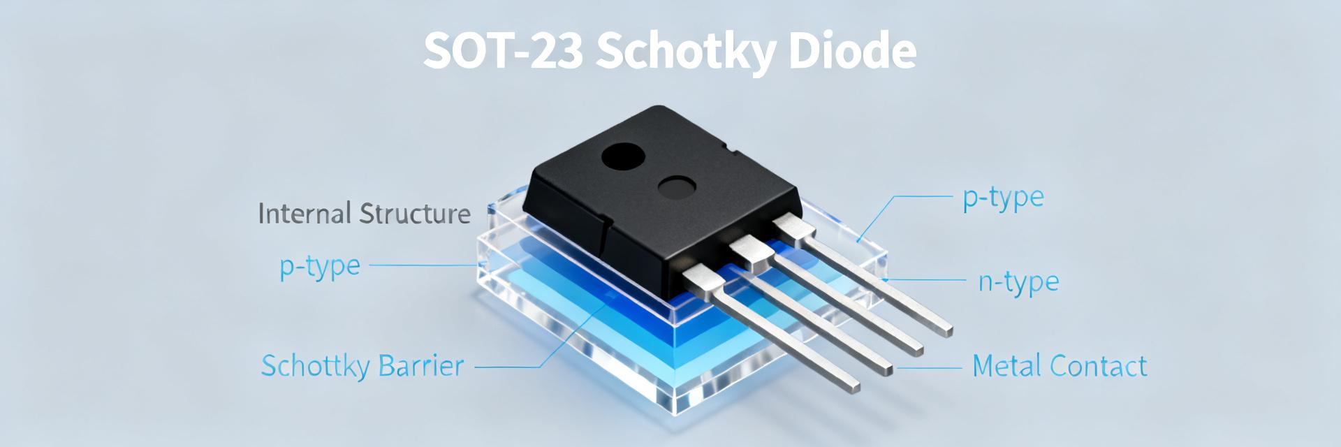
Point: The bas40-07 is a dual small‑signal Schottky diode intended for low‑voltage drop, fast switching, and signal steering uses. Evidence: The package is a compact SOT‑23 style dual diode with common cathode or dual cathode arrangement and short lead lengths to minimize parasitic inductance. Explanation: Typical applications include clamping, reverse‑polarity steering and detection; the datasheet lines that define those uses are VR (reverse voltage), Vf vs IF curves, and Ir vs Vr/T tables.
Quick Specs Summary
Point: Pull a concise spec table from the datasheet and mark values as absolute max or typical. Evidence: The table below highlights the core entries designers check first. Explanation: Use these values as a baseline for design checks and for defining bench test points.
| Parameter | Value (typ/max) | Note |
|---|---|---|
| Repetitive reverse voltage (VR) | ≈ 40 V (absolute max) | Absolute maximum rating |
| Continuous forward current (IF) | ≈ 100–120 mA | Typical DC class; check derating |
| Forward voltage (Vf) | ~0.25 V @1 mA; ~0.45 V @10 mA | Use curve for exact values |
| Reverse leakage (Ir) | μA to nA scale | Rises significantly with Vr & T |
| Max junction temp (Tj) | ≈ 150 °C (absolute) | Design limit |
| Thermal resistance RthJC | Tens to 100 K/W (typ) | Package dependent |
(2) Key datasheet numbers explained
Forward Characteristics
Point: Forward voltage defines power loss and logic threshold margins. Evidence: Vf vs If plots in the datasheet show a low Vf at microamp to milliamp range and a rising slope above tens of milliamps; typical Vf at 10 mA is often ~0.4–0.5 V. Explanation: For power dissipation compute P = Vf × IF; at 50 mA and Vf ≈ 0.6 V the device dissipates ~30 mW, but junction rise depends on thermal resistance — validate with measured Vf at the operating current.
Reverse and Leakage Behavior
Point: Reverse leakage is the most behaviorally variable spec and often rules in signal and pull‑up circuits. Evidence: Datasheet curves show Ir increasing exponentially with temperature and roughly exponentially with Vr; typical values at 25°C are low but can increase by orders of magnitude at higher Tj. Explanation: For high‑impedance inputs assume worst‑case leaked current from the guaranteed max Ir at your Vr and T, or measure several parts across temperature to set pull‑up resistor values.
Vf vs If (schematic sketch):
   Vf
    |
 0.8|          /
    |         /
 0.4|  ------        typical knee near 1-10 mA
    | /
 0.0+----------------- If
     0   1  10  50 mA
(3) Absolute limits & real-world derating
Point: Absolute ratings are not continuous operating targets; they are safety ceilings. Evidence: VRRM = ~40 V, Tj max about 150 °C and non‑repetitive surge specs in the datasheet define short pulse survival. Explanation: Design using derated continuous currents (e.g., operate at 50–70% of IF rating) and treat surge specs as single‑pulse lab conditions — qualify in your intended thermal environment.
Point: Junction temperature rise controls continuous current capability. Evidence: Use RthJA or RthJC from the datasheet and compute ΔT = P × Rth to estimate junction rise; example: at IF=50 mA and Vf=0.5 V, P≈25 mW. Explanation: With RthJA ~150 K/W (package dependent), ΔT≈3.8°C; if RthJA is larger on a small pad, temperature rise increases — increase copper area to lower RthJA or reduce continuous current.
(4) Circuit design & application guidance
Point: Match circuit topology to the controlling datasheet parameters. Evidence: In clamp or steering roles, VR and surge rating define safe headroom; in detection/level shifting VF accuracy and leakage control thresholds. Explanation: For a pull‑up node design, size the pull‑up so that Ir_max × Rpullup produces acceptable voltage error, and verify Vf at the expected IF for threshold comparisons.
Point: Conservative derating and layout reduce field failures. Evidence: Recommended practice: run continuous current at ≤ 70% of the datasheet continuous rating, place diodes close to the clamp node, and provide adequate copper thermal relief. Explanation: Short traces limit parasitic inductance for transient events and copper pours reduce junction temperature; note orientation so thermal paths use the pad and adjacent copper.
(5) Measurement checklist & bench validation
Point: Reproduce key curves under controlled conditions. Evidence: Measure Vf by sourcing stable current (1 mA, 10 mA, 50 mA) with four‑wire sense, and measure Ir with a precision picoammeter at selected Vr values; for temperature sweeps use a controlled thermal chamber. Explanation: Use short fixture leads, note sense lead placement, and avoid self‑heating—allow stabilization time between steps and log ambient and chuck temperature.
Point: Document measured vs datasheet curves and statistical spread. Evidence: Publish Vf vs If, Ir vs Vr at 25°C and an elevated temperature, and a table of worst-case numbers across several lots. Explanation: Record sample size, measurement setup, and any deviations; use tolerance bands (±) to inform design margins and BOM notes for leakage‑sensitive circuits.
(6) Sourcing, substitutes, and a practical design checklist
Point: Substitute selection must be parameter‑led. Evidence: Create a matrix comparing VR, IF continuous, Ir at operating Vr/T, Vf at key IFs, thermal resistance and package geometry. Explanation: Prioritize matching Ir at your operating voltage and temperature, then Vf at the expected currents, and confirm package lead form for thermal and layout compatibility.
Point: A short pre‑production checklist closes the loop. Evidence: Include measured key curves, thermal validation, surge pulse tests and assembly verification. Explanation: Record lot traceability and test results in the BOM; ensure alternate approved parts are listed with matching key specs for supply chain resilience.
Frequently asked questions
What are the critical bas40-07 datasheet specs to verify for a clamp application?
Point: Clamp applications need VR, IFSM, Vf and Ir checks. Evidence: Ensure VR margin for expected transient voltages, confirm non‑repetitive surge capability for expected events, and measure Vf at clamp current levels. Explanation: Also verify thermal path so that repeated clamping doesn’t raise Tj beyond safe limits; log results to BOM for field traceability.
How should I measure reverse leakage for designer decisions?
Point: Use a picoammeter and controlled voltage steps. Evidence: Measure Ir vs Vr at 25°C and at an elevated temperature representative of the application, allow stabilization, and use multiple samples. Explanation: Base pull‑up sizing and high‑impedance thresholds on the worst‑case guaranteed or measured Ir, not on a single typical curve.
What PCB layout changes reduce junction temperature for continuous currents?
Point: Increase copper area and minimize thermal bottlenecks. Evidence: Expand pad copper, connect to internal planes, and minimize solder mask over thermal pads; short traces reduce parasitic inductance for surge events. Explanation: Recompute RthJA after layout changes and remeasure junction rise under the intended current to validate derating.








