
The report summarizes measured and datasheet-backed signals designers care about when evaluating the LM5013DDAR non-synchronous buck regulator. Tests across a wide input window reveal characteristic input-dip responses, measurable thermal limits on compact PCBs, and clear efficiency tradeoffs across load and switching frequency. The article goal is to provide a reproducible test methodology, analyzed results for input behavior, thermal performance and efficiency, and an actionable design and test checklist for engineers.
1 — Background & key specifications to reference (Background)
1.1 Core electrical and package specs to record
Point: Record all nominal device specs before testing. Evidence: datasheet values for input range, max continuous current, allowable junction temperature, selectable switching-frequency ranges, and recommended external component classes. Explanation: For reproducible comparison capture input voltage window, maximum rated load (A), switching-frequency options (kHz), recommended input/output capacitors and catch-diode class, and package thermal characteristics such as junction-to-ambient thermal resistance. These form the baseline for measured vs. datasheet comparisons.
1.2 Test environment & measurement setup
Point: Standardize the lab setup to reduce measurement error. Evidence: use low-inductance scope probes, a calibrated current shunt or power analyzer, an electronic load with fast step capability, an IR camera for steady-state imaging, and K-type thermocouples near the package. Explanation: Specify ambient temperature, PCB copper area, and airflow (CFM or natural convection), keep input ripple within specified limits, and use a solid ground reference. Include a reference netlist and a short schematic snapshot to allow others to reproduce measurements reliably.
2 — Input behavior & transient performance (Data analysis)
2.1 Start-up, minimum input handling and cold-start behavior
Point: Capture soft-start waveform, inrush, and minimum Vin regulation threshold. Evidence: measure Vin, Vout, device input current, and the soft-start node while applying cold-start and hot-start sequences under light and heavy loads. Explanation: Expected signatures include a rounded soft-start ramp when input caps are adequate, a brief inrush that correlates with input capacitance, and a minimum Vin below which regulation collapses. Document start-up under 0.1× and 1× load to show worst-case behavior.
2.2 Response to input dips and near-100% duty operation
Point: Run step/dip tests to characterize hold-up and recovery. Evidence: apply controlled Vin steps of varying depth and duration while logging Vout, duty trace, and device-mode indicators. Explanation: Recommended traces include Vin steps, Vout overshoot/undershoot, and PWM/duty-cycle. Deep or long dips may push the regulator into protection modes or current limit; record recovery time and any latency in soft-start or hiccup that affects downstream systems.
3 — Thermal performance analysis (Data analysis)
3.1 Junction-to-ambient thermal path
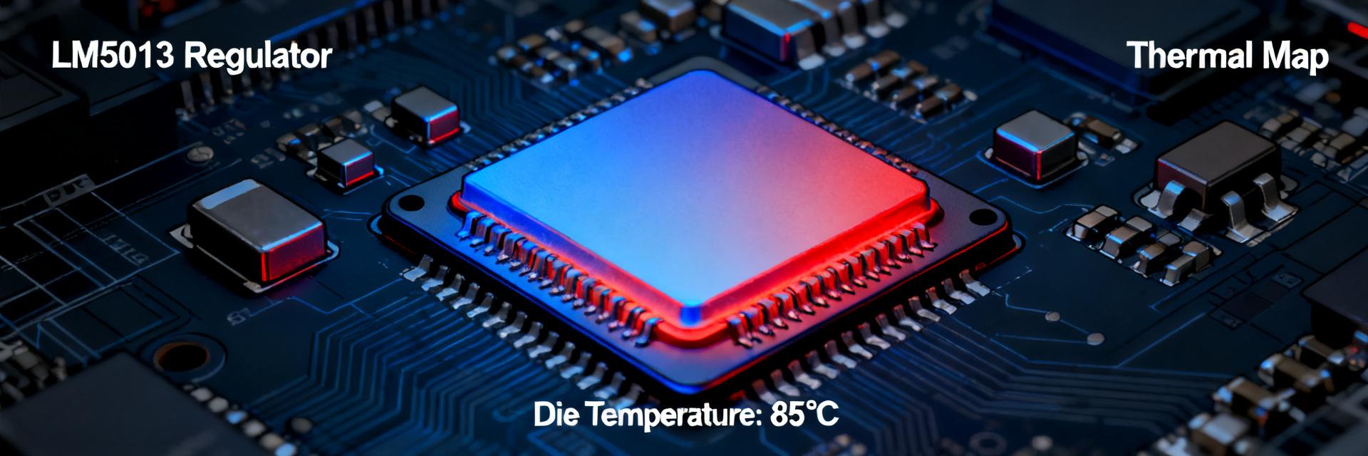
Point: Quantify the thermal path and junction rise with controlled tests. Evidence: steady-state thermal imaging combined with thermocouple junction-adjacent traces provide junction-to-ambient delta-T versus dissipated power. Explanation: Measure PCB copper area, top/bottom pour, and via count; correlate these variables to junction temperature. Use power vs. temperature sweeps to estimate thermal impedance and report both measured junction rise and datasheet thermal-resistance expectations to identify layout-related variance in thermal performance.
3.2 Thermal limiting behavior
Point: Identify how thermal throttling or shutdown appears in data. Evidence: waveform anomalies, sudden efficiency drops, or current limit clamping as case/junction temperature approaches thermal thresholds. Explanation: Thermal limiting typically manifests as reduced switching activity, increased duty-cycle ripple, or eventual shutdown. Document derating guidance, recommended test durations for thermal stabilization, and note reliability impacts of repeated excursions above safe junction limits.
4 — Efficiency benchmarking & loss breakdown (Method & Data)
4.1 Test matrix: Vin, Vout, load points, switching frequency and ambient
Point: Define a representative efficiency test matrix and instrumentation accuracy. Evidence: example matrix—Vin = 12, 24, 48 V; Vout = 5 V; load sweep 0.1 A to 3.5 A; switching-frequency options according to selectable ranges; ambient airflow controlled. Explanation: Calculate efficiency as Pout/Pin using calibrated power instruments, note instrument uncertainty, and sample at steady-state after thermal stabilization. Keep cadence consistent so loss extraction across conditions is comparable.
4.2 Measured efficiency curves and loss-component analysis
Point: Present efficiency vs. load, Vin, and switching frequency and break down losses. Evidence: measured curves should separate conduction, switching, diode/body-diode, and quiescent losses derived from differential measurements and targeted switching-node captures. Explanation: Use synchronous plots and calculations to attribute losses: conduction from I²R and DCR, switching from dv/dt and di/dt product estimation, diode loss from forward recovery, and quiescent from device standby current. This supports targeted optimizations for higher efficiency at the dominant operating point.
5 — Real-world PCB implementation case study (Case study)
5.1 Example design: 12V→5V @ up to 3A — layout and BOM considerations
Point: Show a practical 12→5V @ 3A layout and component choices in neutral terms. Evidence: provide a high-level schematic snapshot and recommended component classes: low-DCR inductors sized for thermal margin, a fast-recovery catch diode class, low-ESR input and output capacitors, and a sense-resistor placement. Explanation: Emphasize primary current-loop minimization, input cap proximity, thermal copper pours, and via stitching near the package to improve both thermal performance and efficiency on small PCBs.
5.2 Measured results vs predicted/simulated performance
Point: Compare predicted losses and thermal profile to measured results and annotate differences. Evidence: tables of predicted vs. measured loss components, thermal images marking hot spots, and efficiency curves overlayed with simulation. Explanation: Typical discrepancies arise from underestimated trace DCR, suboptimal via thermal conductance, or diode recovery effects. Include "what to change next" notes such as increasing copper, selecting a lower-DCR inductor, or relocating the sense resistor to reduce parasitic heating.
6 — Design & testing checklist: actions to improve thermal performance and efficiency (Actionable)
6.1 Thermal mitigation checklist
Point: Provide prioritized thermal fixes and measurement validation steps. Evidence: quantify copper area per watt targets, recommended via count and placement patterns, and forced-air vs. natural convection thresholds. Explanation: Typical recommendations include allocating a minimum copper pour area per watt dissipated, placing thermal vias under and around the package, removing thermal reliefs on primary heat paths, and validating with IR imaging plus a thermocouple at a predefined location after a steady 30–60 minute power soak.
6.2 Efficiency optimization checklist & test plan
Point: Offer concrete efficiency tuning steps and acceptance criteria. Evidence: tradeoffs such as switching frequency selection versus inductor size and loss, selecting lower-DCR inductors and wider traces to reduce conduction loss, and using appropriate snubbers or RCD networks for switching-loss control. Explanation: Include final acceptance tests — efficiency at key load points within targeted delta of prediction, and thermal stability defined as








