
The introduction highlights the part number, datasheet references, and measured performance expectations engineers need when specifying robust links for sensors, controllers, and building automation nodes. These values set the baseline for test setups, termination strategies, and qualification checklists used during board bring‑up and field validation.
Product Overview & Key Features (Background)
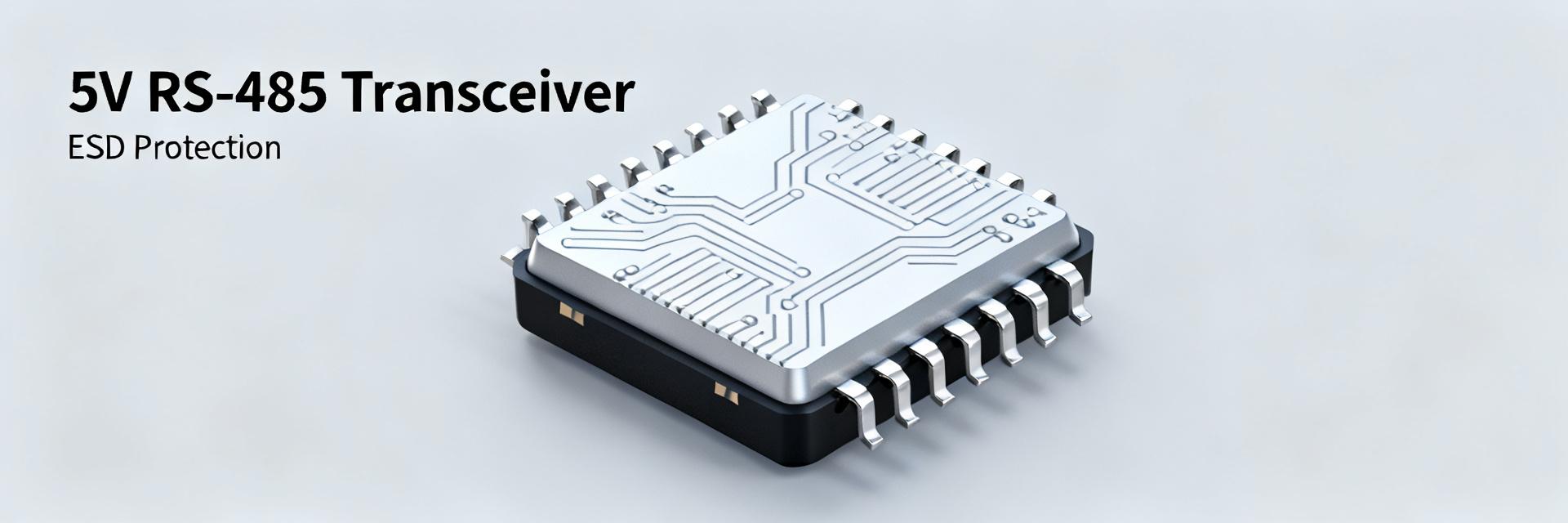
Device description & package
This device is a half‑duplex RS‑485/RS‑422 transceiver with automatic direction control suitable for multi‑drop industrial links. It comes in an 8‑pin SOIC (NSOIC) footprint, supporting space‑constrained embedded designs and compact field modules. Quick specs for fast review: recommended VCC 4.75–5.25 V, max data rate 500 kbps, ESD protection ±15 kV, operating temperature −40 °C to +85 °C.
Core safety & robustness highlights
The transceiver integrates multiple protections that influence long‑term field reliability: high‑level ESD immunity, fail‑safe receiver behavior (bus open/short/idle), wide common‑mode input range, and receiver hysteresis to reject noise. These elements reduce false‑trips and post‑installation failures, particularly in electrically harsh industrial environments and when paired with proper board layout and connector handling.
Electrical Specifications & Absolute Limits (Data Analysis)
Recommended operating conditions vs absolute maximums
Recommended operating conditions (from the datasheet) center on VCC = 4.75–5.25 V and ambient operation between −40 °C and +85 °C. Input and output thresholds follow TTL/CMOS‑compatible levels when VCC is within that window. Absolute maximums for stresses (transient voltages, storage temperatures, and pin‑to‑pin ratings) are listed in the datasheet; consult those tables before margining for surge or single‑event transients in the field.
| Parameter | Value (Typical) | Conditions |
|---|---|---|
| Supply Voltage (VCC) | 5.0 V | Standard Ops |
| Receiver Hysteresis | 25 mV | Noise Rejection |
| Data Rate | 500 kbps | Max Guaranteed |
Key electrical parameters to monitor
Critical parameters for design decisions include supply current (typical and worst‑case), driver differential output swing into standard loads, receiver hysteresis (~25 mV typical), slew rate limits, and propagation delays. Measure these at VCC = 5.0 V, RL = 54 Ω (or bus equivalent), and room temperature, and rerun at temperature extremes to validate worst‑case timing and power.
Performance Characteristics & Benchmarks (Data Analysis)
Data-rate, signal integrity & timing benchmarks
The datasheet lists a 500 kbps practical upper limit for reliable signaling on balanced twisted‑pair cabling. Verify with scope captures: use a 100 MHz–200 MHz scope, 1 GS/s or higher, 10× probes, and differential probe or transformer coupling. Capture eye diagrams and timing traces for propagation delay, rise/fall times, and enable/disable timing under nominal and loaded conditions to reproduce datasheet figures.
Robustness tests: ESD, common-mode & fault conditions
ESD immunity at ±15 kV (air/contact) is a headline spec—run IEC/ANSI‑equivalent contact and air discharges during qualification. Test common‑mode tolerance with offsets across the recommended common‑mode range and apply controlled short‑to‑ground or VCC faults per the datasheet. Log voltage/current waveforms, and document any deviation from expected recovery or fail‑safe behavior for root‑cause analysis.
Integration & Board-Level Design Guidelines (Method)
Recommended termination, biasing & network topology
Use a matched differential termination (typically 120 Ω across A/B for long runs) at each line end and implement fail‑safe biasing with pull resistors that hold the bus in a defined idle state. For multi‑node networks, follow two‑terminator topology with stubs minimized; standard practice is to keep stub lengths under a few centimeters and limit node counts per the system unit‑load budget.
Layout, decoupling & thermal best practices
- Keep differential pairs short and parallel with controlled differential impedance (~100 Ω).
- Place a 0.1 µF ceramic decoupling capacitor as close to VCC pin as possible.
- Use a solid ground plane for return currents and route ESD components near the connector.
- Monitor power dissipation and ensure adequate copper area for thermal management.
Application Examples & Comparative Use-Cases (Case Study)
1. Industrial Sensors
Prioritize robustness and ESD immunity; use 120 Ω terminations and biasing for deterministic idle states.
2. Building Automation
Balance cable length vs data rate—lower bitrates increase reach across large trunks.
3. Embedded Controller
Compact SOIC package favors tight layouts; prioritize automatic direction control for simplified firmware.
How to choose this transceiver vs generic alternatives
Use an objective rubric: score candidates on ESD level, fail‑safe behavior, operating temperature, data‑rate headroom, supply compatibility, and auto‑direction convenience. Weight reliability and ESD higher for field deployments; choose devices with documented hysteresis and common‑mode ranges when bus noise is a common failure mode.
Troubleshooting & Testing Checklist (Action)
Pre-deployment test checklist
- Continuity and connector pinout verification.
- VCC stability validation (
- Eye diagram timing checks at target bitrate.
- ESD handling procedure and recovery behavior documentation.
Common failure modes & fixes
Noisy bus: add common‑mode chokes or increase receiver hysteresis; missing data: confirm terminations and biasing; intermittent issues after ESD: relocate TVS/ESD suppression closer to connector and add ground return paths.
Summary
The MAX13487EESA+T targets robust 5 V RS‑485/RS‑422 half‑duplex links with a practical data rate of 500 kbps, strong ESD protection, and industrial temperature support.
- Design around the recommended VCC 4.75–5.25 V and bound thermal design.
- Validate timing and signal integrity with differential eye diagrams.
- Prioritize board layout and ESD suppression placement to protect sensitive nets.








