
A technical synthesis of datasheet performance, lab validation, and integration strategies.
The HMC735LP5E VCO delivers a 10.5–12.2 GHz tuning band with datasheet figures and independent lab measurements showing competitive close-in phase noise and bias-dependent output power. This report synthesizes the datasheet fields engineers must track, contrasts expected lab behavior with published numbers, and provides a reproducible measurement recipe plus integration tactics to maximize usable output while protecting phase noise performance.
1 Device background & must-track specs
1.1 Key electrical specs to call out
Point: Compare a concise set of electrical fields from the latest datasheet to predict phase noise and output power behavior. Evidence: extract frequency range, tuning sensitivity (MHz/V), Vcc and typical current, divide-by-4 output option, and typical output impedance. Explanation: these fields directly influence VCO tuning linearity, noise contribution from bias networks, available drive, and load sensitivity — all critical when assessing phase noise and fundamental level for system design.
| Spec | Typical Units | Why it matters |
|---|---|---|
| Frequency range | GHz | Determines tuning band where phase noise is specified |
| Tuning sensitivity | MHz/V | Links control voltage noise to frequency jitter |
| Supply V/I | V, mA | Sets noise contribution and thermal power dissipation |
| Output option (÷4) | Yes/No | Lower output level and different spectral purity |
| Output impedance | Ω | Guides matching network to prevent load pulling |
1.2 Package, pinout and typical application contexts
Point: Mechanical and thermal details affect long-term stability and output performance. Evidence: note package style, thermal pad presence, and recommended footprint from the datasheet. Explanation: a solid thermal pad and low-impedance ground return reduce junction temperature and flicker-related drift; typical applications such as LOs for narrowband receivers, up/down converters, and test-sources dictate whether phase noise or raw output power is the primary selection criterion.
2 Phase noise & output power: datasheet numbers vs expected lab behavior
2.1 Phase noise breakdown by offset and frequency
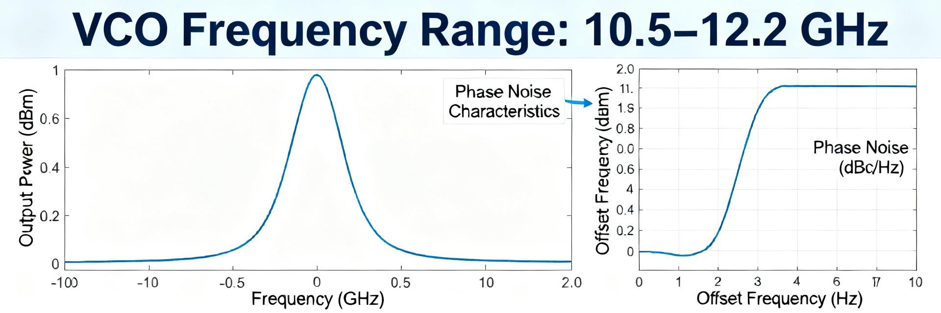
Point: Report phase noise at standard offsets to allow apples-to-apples comparison. Evidence: extract or measure values at 100 Hz, 1 kHz, 10 kHz, 100 kHz and 1 MHz offsets and plot on a log scale. Explanation: close-in offsets reveal tuning voltage and bias-related noise, mid offsets show device flicker and device intrinsic noise, while far offsets approach device thermal noise; expect variation across the tuning band and small bias changes, so present curves at multiple center frequencies.
2.2 Output power characteristics and harmonic content
Point: Characterize fundamental level and harmonics vs frequency and bias. Evidence: tabulate fundamental dBm vs frequency across the band and vs supply/bias; report second harmonic and any spurious tones and note any difference when using the divide-by-4 output. Explanation: output power typically shifts with bias and load; harmonics and spurs indicate nonlinearity and matching issues — report fundamental level, harmonic suppression (dBc) and, if available, P1dB or IP3 to quantify usable drive.
3 How to measure phase noise and output power correctly (method guide)
3.1 Test setup and required instrumentation
Point: A minimal, well-instrumented bench is required for repeatable results. Evidence: use a low-noise DC supply with good filtering, 50 Ω matched probe or connector, a phase-noise-capable spectrum analyzer or phase noise analyzer, calibrated power meter, and fixed attenuators/isolation. Explanation: ensure 50 Ω termination, use isolation to avoid load pulling, correct for cable loss and analyzer noise floor, and control temperature to reduce drift during multi-point sweeps.
3.2 Measurement procedure and best practices
Point: Follow a stepwise recipe and record settings for reproducibility. Evidence: bias and warm-up, tune to target frequencies, measure phase noise at standard offsets, capture output power and harmonics, and sweep bias points; record RBW/VBW, detector type, averaging and calibration steps. Explanation: document analyzer noise floor and subtract it where supported, watch for connector reflections and use isolation amplifiers if the DUT drives the analyzer into nonlinearity, and repeat measurements to quantify variability.
4 Comparative evaluation & selection criteria (case study)
4.1 Benchmarking metrics and presentation
Point: Normalize metrics to compare the device against peer MMIC VCOs in the 10–12 GHz band. Evidence: overlay phase noise vs offset for given bias points, chart output power vs frequency under identical load and supply, and compute phase-noise per MHz of tuning. Explanation: normalized plots reveal whether the VCO’s phase noise advantage is preserved across the band or only at specific frequencies, and whether output power requires buffering to meet system-level gain and linearity.
4.2 When to choose this VCO: trade-offs and application fit
Point: Match device attributes to system requirements. Evidence: evaluate scenarios such as narrowband LO where close-in phase noise dominates, versus distributed transmitter chains where output power and harmonic suppression matter more. Explanation: choose this VCO when its phase noise profile meets receiver sensitivity or PLL phase noise budget; otherwise plan buffering, filtering, or alternate parts if raw output or spur levels are insufficient.
5 Integration & optimization checklist (actionable recommendations)
5.1 PCB, biasing and RF chain tactics to improve phase noise and output power
Point: Layout and biasing have first-order impact on both metrics. Evidence: implement coplanar ground, short RF traces, a solid thermal pad, multi-stage decoupling on Vcc, and a matched output network. Explanation: low-impedance ground and thermal paths reduce microphonic and thermal flicker; careful matching minimizes reflected power and load pulling, improving measured phase noise and stabilizing output power across the band.
5.2 System-level tips: buffering, PLL use and thermal management
Point: Use system elements to preserve VCO performance under load. Evidence: add a low-noise buffer amplifier when drive or isolation is required, lock with a PLL for long-term stability and improved close-in noise, and plan thermal derating or heat sinking. Explanation: buffering prevents load pulling and enables constant-load measurements; PLLs move phase noise to within loop bandwidth while preserving far-offset performance; thermal control reduces drift over time.
Summary
The HMC735LP5E VCO datasheet sets expectations for phase noise and output power, but validated performance depends strongly on bias, matching and the measurement approach. Use the checklist, repeatable measurement recipe, and normalized plots to confirm the device meets your system trade-offs before committing to a final BOM and RF chain.
- Focus on the datasheet fields listed above—frequency range, tuning sensitivity, supply V/I and output impedance—to anticipate phase noise sensitivity and output power under load; verify with swept measurements.
- Measure phase noise at standard offsets (100 Hz–1 MHz) and plot curves at multiple tuning points to reveal bias and tuning voltage effects; compare normalized curves to peers.
- Control matching and grounding on the PCB, add buffering when needed, and document measurement settings (RBW/VBW, averaging) to ensure reproducible output power and phase noise results.
Frequently Asked Questions
How should I measure HMC735LP5E VCO phase noise at 1 MHz offset?
Use a phase-noise-capable analyzer or a spectrum analyzer with a PN option, ensure a stable, low-noise supply, warm up the device, tune to the target frequency, and record the noise at 1 MHz offset with RBW/VBW and averaging logged; correct for analyzer noise floor if required.
What is the best way to report HMC735LP5E output power vs frequency?
Report fundamental dBm across the tuning band at a fixed supply and load (50 Ω), include harmonic levels in dBc, and annotate any divide-by-4 output differences; present a table or chart so designers can assess buffering needs.
How can bias and matching influence HMC735LP5E phase noise?
Bias ripple and poor decoupling introduce control-voltage and supply noise that downconverts to phase noise; mismatched loads cause load pulling and frequency jitter. Mitigate with multi-stage decoupling, clean regulation, and a matched output network to preserve phase noise performance.








