
A direct comparison of published datasheet figures and independent bench measurements reveals where the ad623arz meets expectations — and where practical performance differs.
This article unpacks the manufacturer datasheet claims, presents reproducible measurement methods and practical design advice so engineers can verify gain accuracy, noise, and thermal behavior with confidence.
1 — Product overview & datasheet at-a-glance (background)
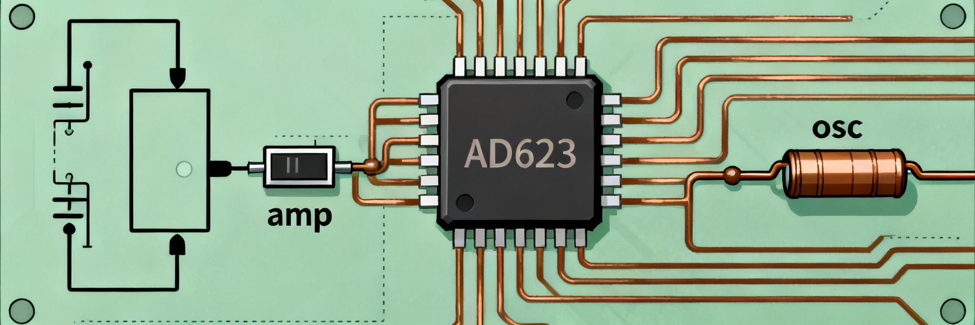
1.1 Key electrical specifications (direction)
Point: The published datasheet lists headline electrical specs that set expectations for single-supply instrumentation applications.
Evidence: Typical and maximum values are provided for supply range, input/output behavior, offset, noise, CMRR, bandwidth and output swing.
Explanation: The table below organizes those claims so engineers can directly compare to measured results under defined test conditions.
| Parameter | Typical | Limit/Max | Units |
|---|---|---|---|
| Supply voltage range | +2.7 to +12 | ± (as specified) | V |
| Rail-to-rail I/O | Yes (typical) | Output swing to within ≈100–200mV | V |
| Gain set | Single RG resistor | - | - |
| Input offset | ~25 μV typ | 250 μV max | μV |
| Input noise (RMS) | ~8 nV/√Hz | - | nV/√Hz |
| CMRR (G=1) | ~110 dB typ | >80 dB spec | dB |
| Bandwidth (G=1) | ~1.2 MHz | - | MHz |
1.2 Package, pinout and target applications (direction)
Point: The device is offered in compact SOIC/SOT packages optimized for space-constrained front ends.
Evidence: Datasheet pin diagrams identify power, IN+, IN−, RG and output pins and recommend routing for low-noise paths.
Explanation: Designers should consult the datasheet pinout diagrams when placing RG and differential inputs to minimize trace capacitance and preserve CMRR in sensor front-ends and data-acquisition chains.
2 — Absolute ratings, operating conditions & thermal constraints
2.1 Absolute maximums and recommended operating ranges (direction)
Point: Staying within absolute maximums and recommended ranges prevents latent failures and preserves performance. Evidence: The datasheet specifies absolute voltage limits, recommended supply range and temperature handling and ESD ratings. Explanation: Engineers should verify supply headroom, avoid injecting inputs beyond specified common-mode limits, and respect ESD/handling guidance during PCB assembly and test to maintain long-term reliability.
2.2 Thermal performance and derating guidance (direction)
Point: Thermal derating ties electrical operation to PCB design. Evidence: Using published thermal resistance and supply current, one can compute junction temperature rise for given ambient and power dissipation. Explanation: Calculate Pd = Vsupplied × Iq + dynamic output drive contributions; apply θJA from the datasheet and add PCB copper to reduce θJA. Expect modest case rises under light loads, but plan for worst-case output swing and high ambient when qualifying boards.
3 — Electrical performance: datasheet specs vs. bench performance
3.1 Gain accuracy, offset, drift & CMRR (direction)
| Parameter | Datasheet (typ/limit) | Measured (example) | Test conditions |
|---|---|---|---|
| Gain error (G=10) | ±0.1% typ / ±0.5% max | ±0.3% | Vsup=5V, Ta=25°C, RG=11.9k |
| Input offset | 25 μV typ / 250 μV max | 70 μV | Same as above |
| CMRR (G=10) | 80–110 dB | ~85 dB | Diff source with 1V CM |
Note: Measured deviations often correlate with RG tolerance and layout constraints.
3.2 Noise, bandwidth, slew rate and settling time (direction)
Point: Measured noise and bandwidth depend strongly on instrument bandwidth, input source impedance and layout. Evidence: Datasheet noise is given as nV/√Hz and bandwidth as −3 dB points; bench RMS noise will differ with filter and probe loading. Explanation: Report RMS noise over a specified bandwidth, specify −3 dB bandwidth and include probe/load details; mitigate excess noise with local filtering and low source impedance.
4 — Measurement Methodology
Test Setup: Use low-noise DC supply (
Analysis: Capture raw waveforms at ≥10× bandwidth. Report offset as mean, noise as RMS over stated bandwidth.
5 — Design Checklist
- Short RG traces & adjacent input routing.
- Star ground and stitched ground planes.
- Low-TCR RG with 0.1% tolerance.
- Avoid heavy capacitive output loads.
6 — Deployment & Real-World Example
6.1 Example: single-supply sensor front-end
Verify that the amplifier’s output swing covers ADC input range with headroom. Calibrate offset in firmware if required. SNR improvements are usually proportional to gain.
6.2 Quick action checklist (Prototyping to Production)
- ✓ Validate offset and noise at target gain.
- ✓ Perform thermal check with worst-case drive.
- ✓ Finalize PCB layout with proper bypassing.
- ✓ Set acceptance criteria before sign-off.
Key Summary
- The published datasheet sets clear expectations; verify these under your exact gain and supply to ensure ad623arz references.
- Thermal and layout factors cause the largest divergence; use the decoupling and grounding checklist.
- Use reproducible test setups: record ambient, supply, RG, and probe type for repeatable data.
Frequently Asked Questions
What are the typical datasheet vs measured offset expectations?
Expect typical bench offsets to be higher than the ideal datasheet typical due to RG tolerances, input bias currents and temperature. Use tighter RG or software calibration if needed.
How should noise be reported when validating datasheet claims?
Report RMS noise over a specified −3 dB bandwidth with instrument settings documented. State the input source impedance as it affects measured results.
What layout steps most effectively improve measured CMRR and noise?
Keep differential traces equal, place RG adjacent to pins, use local bypass caps, and separate analog from noisy digital return paths.
Summary
The manufacturer datasheet provides the baseline specs, but layout, thermal, and test conditions create divergence. Reproducible methodology and disciplined layout are key to matching datasheet claims.
Call-to-action: Follow the test setup and checklists above before committing to production.








