
The MAX31865 is presented as a high-resolution RTD-to-digital interface offering 15-bit conversions for precision temperature measurement. This introduction frames why 15-bit resolution matters: finer quantization, smaller LSB step, and improved ability to resolve sub-0.1°C changes in instrumentation and industrial designs while keeping system complexity modest.
This concise, bench-driven technical overview outlines the device's core specs, pinout and wiring guidance, SPI/register basics, recommended bench test methodology, representative observations, and practical integration tips for confident deployment in measurement systems.
Quick Overview & Key Specs
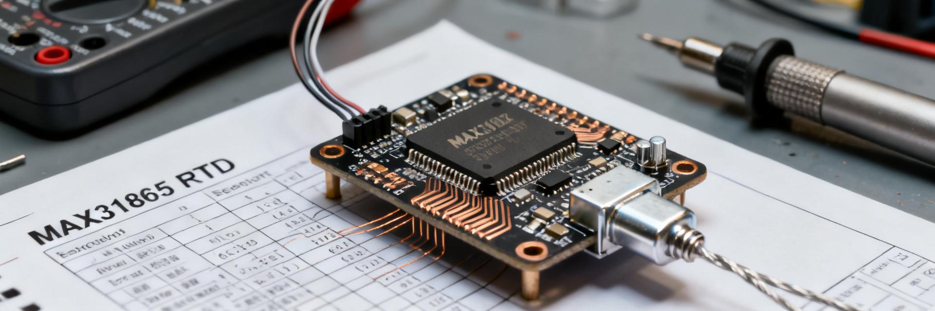
What the MAX31865 Does
Point: The device converts RTD resistance (PT100/PT1000) to digital counts via an internal ADC.
Evidence: It supports 2-, 3-, and 4-wire RTD topologies and relies on an external reference resistor to set excitation.
Explanation: Designers use the converter to remove bridge circuitry, leveraging integrated excitation, fault detection, and digital output to simplify temperature acquisition.
High-level Electrical & Performance Specs to Cover
Point: Key datasheet metrics determine suitability for a design.
Evidence: Extract supply range, recommended reference resistor range, ADC resolution, conversion modes and timing, input protection, and fault-detection behavior.
Explanation: Emphasize excitation current, conversion latency, and operating temperature range since these directly affect measurement noise, settling, and system calibration strategies.
Pinout & Hardware Connections (pinout)
Pin Functions & Signal Descriptions
Point: Group pins by function for clarity.
Evidence: Typical groups include SPI (SCK, MOSI, MISO, CS), RTD inputs (RTD+, RTD−, bias/sense), reference resistor node, VCC, GND, and FAULT/STATUS.
Explanation: Describe safe I/O voltage levels, place decoupling close to VCC, and size I/O drive to meet SPI timing while protecting high-impedance RTD sense nodes from leakage and noise.
Wiring for 2-, 3- and 4‑Wire RTDs
Point: Wire topology affects compensation and accuracy.
Evidence: 2‑wire is simplest but worst for lead-resistance error; 3‑wire uses a third lead to cancel lead resistance; 4‑wire provides the best compensation.
Explanation: Recommend minimizing lead length, use twisted pair or shielded cable, and route sense wires away from heat sources; place sense returns near the device to reduce common-mode errors.
SPI Interface & Register Basics
Key Registers & Configuration Bits to Explain
Point: Registers control conversion and report results.
Evidence: Document configuration/control register, MSB/LSB conversion result registers, and fault-status registers; note read/write rules like auto-increment and multi-byte reads.
Explanation: Explain bits for conversion mode, filter settings, bias enable, and fault toggles; recommend conservative defaults (bias enabled, continuous or single-shot per application) for predictable behavior.
Timing, Data Rates & Communication Best Practices
Point: Correct SPI timing yields reliable reads.
Evidence: Observe maximum SCK frequency, CS setup/hold requirements, and conversion-read sequencing in the datasheet.
Explanation: Use a dedicated SPI transaction for conversion reads, allow required settling after enabling bias, avoid bus contention with chip-select gating, and capture logic traces when debugging timing-related errors.
Bench Test Methodology
Recommended Test Setup
Point: A controlled bench reduces measurement ambiguity.
Evidence: Use a stable DC supply, low-noise precision reference resistors, calibrated RTD or decade box, short/medium/long lead configurations, oscilloscope and multimeter probes, and an SPI logic analyzer.
Explanation: Allow ambient stabilization and warm-up, and shield the setup to minimize conducted and radiated interference during noise measurements.
Test Procedures & Metrics to Record
Point: Systematic procedures produce repeatable metrics.
Evidence: Steps: verify supply and pin voltages, confirm SPI comms, toggle configuration modes, capture repeated conversions for noise/RMS, and sweep resistance/temperature for linearity.
Explanation: Record LSB RMS noise, linearity/error vs. ideal RTD curve, drift, conversion latency, excitation impact, and fault detection behavior for a comprehensive characterization.
Bench Results: Expected Observations & Troubleshooting
Typical Result Categories to Report
Point: Organize reported results for clarity.
Evidence: Present conversion traces, noise histograms, linearity plots (error vs. resistance/temperature), and responses to deliberate lead resistance changes.
Explanation: Include raw snippets and processed plots with captions summarizing key findings, such as observed RMS noise in LSBs and any nonlinearity or offset requiring calibration.
Common Problems & Fixes Seen on the Bench
Point: Recurrent issues are generally solvable with focused checks.
Evidence: Common root causes include SPI timing mistakes, incorrect reference resistor value, noisy supply, poor grounding, and miswired RTD topology.
Explanation: Diagnose by isolating the RTD from the board, switching to single-shot mode, inspecting fault-status registers, and substituting a known-good precision reference resistor to localize the fault.
Integration Tips & Practical Checklist
PCB, Power, and Layout Recommendations
Point: Layout decisions strongly influence measurement fidelity.
Evidence: Implement short RTD traces, star-grounding, analog/digital partitioning, decoupling capacitors placed close to VCC, and guard traces around high-impedance nodes.
Explanation: Keep heat-generating components away from RTD traces, route sensitive traces on inner layers when possible, and add test points for production verification.
Firmware, Calibration & Production Considerations
Point: Firmware and QA complete a robust solution.
Evidence: Sequence startup to enable bias and allow settling, initialize registers deterministically, implement averaging or digital filtering, and code fault-handling logic.
Explanation: Calibrate scale and offset against standards, verify reference resistor tolerance, include open-circuit detection tests, and add production test vectors for end‑to‑end system verification.
Summary
In short, this technical overview covers the essential approach to evaluating a 15‑bit RTD front end: capture the critical electrical specs, verify correct pinout wiring and SPI/register sequences, run a structured bench program that records noise and linearity, and apply layout and firmware best practices to achieve reliable temperature measurement.
- Confirm key specs: supply range, recommended reference resistor, ADC resolution, conversion modes, and fault detection to ensure design fit and predictable behavior.
- Validate pinout wiring: wire 2/3/4‑wire RTDs per topology, minimize lead length, and apply proper decoupling and grounding for low noise.
- Execute bench tests: log LSB RMS noise, linearity error vs. resistance, conversion latency, and fault behavior; use stable references and shielded setups for trustworthy data.
FAQ
How should one choose the reference resistor value for best accuracy?
Choose a low-drift, precision reference resistor near the target RTD resistance divided by expected gain to set full-scale counts. Verify tolerance and temperature coefficient, and measure its actual resistance during calibration; discrepancies here directly map into scale error and degrade absolute accuracy if uncorrected.
What is the best practice to debug an apparent offset or noise?
Isolate the sensor with a short calibrated resistor, switch to single-shot conversions, verify supply stability and decoupling, inspect SPI timing, and read fault registers. Substituting a known precision reference resistor quickly differentiates board issues from sensor or wiring faults.
Which RTD topology should I use for production installations?
For production, 3‑wire provides a strong compromise between wiring complexity and compensation for lead resistance; 4‑wire is preferred where highest absolute accuracy is required and wiring cost is acceptable. Use 2‑wire only where lead resistance is negligible or calibrated out.








