
Executive Summary: The DS1307 is a timekeeping IC with a 32.768 kHz crystal timebase and 56 bytes of nonvolatile SRAM; designers commonly benchmark RTC choices by standby current, VBAT switchover behavior, and seconds/day accuracy. This article serves as a practical, data-first technical guide for engineers to design, measure, and troubleshoot reliably.
1 — What the DS1307 RTC Is: Overview & Core Features
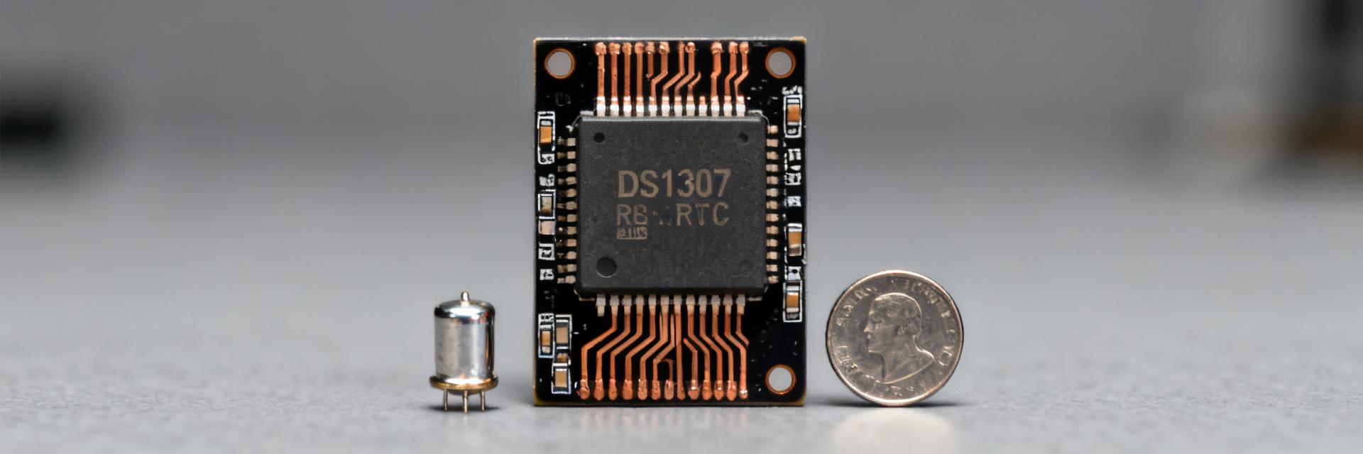
The DS1307 is a serial real-time clock with simple I2C communication and a small nonvolatile RAM for user data. Datasheet values identify the function as a clock/calendar plus 56 bytes of NV SRAM and an I2C-compatible bus, driven by a 32.768 kHz crystal. Its small SRAM and straightforward I2C make it popular in legacy embedded designs where external nonvolatile storage and battery backup are required.
Typical applications and why designers still use it
The DS1307 is used in embedded controllers, low‑power data loggers and legacy product refreshes. Its longevity comes from a simple I2C interface, small parts count and included NV SRAM. Trade‑offs include higher standby current and limited accuracy compared with modern low‑power RTCs, but simplicity, availability in 5V ecosystems and predictable behavior keep it in many BOMs.
2 — Detailed Electrical & Timing Specifications
Understanding supply limits and timing is central to reliable behavior; designers must consult the datasheet for exact limits before layout. The datasheet lists VCC and VBAT operating ranges, absolute maximums and recommended decoupling values. Treat those numbers as design limits and build safe margins in regulators and battery selection.
Supply, voltage ranges and absolute limits
Review the DS1307 voltage rails and protection points to avoid latch‑up or data loss. Follow conservative margins, place solid decoupling on VCC and a local bypass on VBAT, and avoid driving the I/O pins beyond the present supply rail to protect the part.
Timekeeping accuracy, oscillator and calendar behavior
Calculation Note: Timekeeping accuracy is dominated by the crystal tolerance. Convert ppm to seconds/day by multiplying ppm × 86.4; for example, a 20 ppm crystal yields ≈1.7 seconds/day drift (20 × 86.4 = 1,728 counts → 1.728 sec/day).
3 — Power Architecture and Battery Backup Details
The DS1307 uses an internal power‑sense scheme to preserve time when VCC is removed. Datasheet values describe automatic switchover to VBAT and the requirement for a backup source. Design the backup path with a low‑leakage coin cell, include series resistance considerations for inrush, and avoid placing protection diodes that raise VBAT loss thresholds excessively.
VBAT Switchover
Verify switchover timing and signal integrity during VCC dropouts. Recommended checklist: CR2032 cell, secure holder, 0.1 μF bypass on VBAT, and local ground reference.
Current Consumption
Measure at the VBAT pin with system I2C lines idle. Use a low‑noise nanoammeter to capture true standby behavior, isolating leakage by removing sockets.
4 — Interfacing, Register Use & Design Best Practices
Correct register access and robust I2C handling prevent data corruption. The register map reserves addresses for seconds→year, a control register and 56 bytes of SRAM. Implement read/write sequences with ACK/NACK checking and simple retry logic.
I2C register map essentials
Key registers live at byte offsets 0x00–0x06 for time, 0x07 for control and 0x08–0x3F for SRAM. Example flow: write device address + register pointer 0x00, send BCD time bytes, stop; to read, write pointer then restart and read seven bytes.
5 — Troubleshooting, Validation Checklist & Alternatives
Validation Checklist
- Confirm VCC and VBAT voltages and measure switchover during a controlled power drop.
- Measure oscillator frequency and amplitude with a scope; compare to 32.768 kHz target.
- Read time registers over I2C to confirm values and check SRAM integrity.
- Evaluate environmental influences: temperature swings and mechanical stress on crystal.
Summary
- DS1307 provides a simple I2C RTC with 56 bytes NV SRAM; use datasheet values for VCC/VBAT limits.
- Power design should validate VBAT switchover and include local decoupling.
- Timing accuracy is crystal-dependent; budget drift based on ppm ratings.
- Interfacing requires BCD register handling and careful PCB layout around the oscillator.
- Troubleshoot by verifying rails, oscillator waveforms, and register integrity.
Final note: this data‑focused guide helps turn datasheet values into verified design decisions. DS1307, RTC, specs.
Frequently Asked Questions
What is the DS1307 VBAT switchover behavior?
The device automatically switches to the backup supply when main VCC is absent. Validate switchover on the bench by capturing VCC and VBAT traces during an induced VCC collapse and confirm the time registers continue counting.
How accurate is the DS1307 timekeeping?
Accuracy is set by the external 32.768 kHz crystal and its tolerance/temperature drift. Calculate drift as ppm × 86.4 to convert to seconds/day and select a crystal appropriate for your application.
What test methods verify DS1307 power consumption specs?
Use a precision nanoammeter or source‑measure unit and log currents over time for stable averages. Measure at the power pin with I2C idle, isolate leakage, and average measurements to remove switching noise.








