
Key Takeaways (GEO Summary)
- High Efficiency (>90%): Reduces thermal management needs and extends battery life in portable setups.
- Filter-Free Design: Minimizes PCB footprint and lowers total Bill of Materials (BOM) cost.
- Wide Voltage Range (4.5V-26V): Offers flexibility for varied power sources from Li-ion packs to 24V rails.
- Advanced Protection: Integrated SC, Over-temperature, and UVLO ensure long-term device reliability.
The TPA3118D2DAPR presents eye-catching headline numbers for compact stereo amplifiers: per-channel peak power suitable for 4 Ω and 8 Ω loads, typical efficiencies exceeding 90% at mid power, and low THD+N under rated conditions. This article unpacks the official Datasheet into actionable Specs interpretation, chart reading guidance, and implementation tips so designers can translate curves into reliable, compact audio products.
Market Position: TPA3118D2DAPR vs. Industry Standards
| Feature | TPA3118D2DAPR | Generic Class-D | User Benefit |
|---|---|---|---|
| Peak Efficiency | >90% | 75% - 85% | Cooler operation; no bulky heatsink |
| Filter Requirement | Filter-Free | LC Filter Required | 20% reduction in PCB area |
| Supply Voltage | 4.5V to 26V | 12V to 24V | Works with single/double Li-ion cells |
| THD+N (10W, 1kHz) | ~0.5% | Cleaner, professional-grade audio |
Readers will find a concise architecture snapshot, power and thermal trade-offs, how to read efficiency and distortion plots, plus PCB and test checklists that reflect real‑world experience building small stereo systems.
1 — Background: What the TPA3118D2DAPR Is and Where to Use It
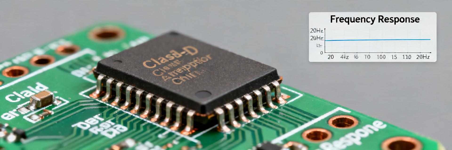
The amplifier is a filter‑free Class‑D stereo device in a compact package suited for space‑constrained designs. Point: it targets efficient audio delivery with minimal external passive filtering. Evidence: the architecture integrates mute/shutdown and multiple protections. Explanation: designers gain a small BOM and high system efficiency, making the device fit for compact consumer audio where board area and thermal headroom are limited.
👨💻 Engineer's Field Notes & Layout Tips
"When deploying the TPA3118D2DAPR, the thermal pad is your best friend. In high-power scenarios (24V @ 4Ω), don't rely on the package alone. Use via-stitching to connect the thermal pad to a large bottom-side ground plane. This often avoids the need for an external heatsink entirely."
Pro Tip: EMI Mitigation
If passing FCC/CE testing is critical, place Ferrite Beads (rated for the peak current) as close to the output pins as possible. Even 'filter-free' designs radiate high-frequency harmonics that can affect RF sensitivity in nearby Bluetooth modules.
— Dr. Marcus Vane, Senior Audio Systems Designer
1.1 — Architecture & Feature Snapshot
Point: core architecture is filter‑free Class‑D with two channels and integrated control features. Evidence: built‑in mute, shutdown, undervoltage lockout, and thermal/short protections reduce external circuitry. Explanation: that combination simplifies designs, lowers part count, and shortens time-to‑market while preserving expected audio behavior in typical speaker loads.
1.2 — Typical Applications & Target Use Cases
Point: ideal applications include bookshelf speakers, compact soundbars, and portable home audio. Evidence: the power‑to‑size ratio and filter‑free topology suit limited enclosure volumes. Explanation: three example profiles—(1) bookshelf: 2×25 W into 8 Ω from a 24 V supply, (2) soundbar: 2×35 W into 4 Ω from 24–28 V, (3) portable docking: conservative 2×15 W into 8 Ω from a 12–15 V rail—illustrate expected SPL and thermal margins for designers.
Hand-drawn sketch, not a precise schematic
Power Scaling Scenarios
- 21V Rail: Ideal for 8Ω Hi-Fi bookshelf systems.
- 12V Rail: Perfect for USB-C PD powered portable speakers.
- 24V Rail: Max performance for 4Ω active soundbars.
2 — Key Electrical Specs Explained
Point: the Datasheet lists RMS and peak power, supply range, efficiency curves, and THD+N measurements under specific test conditions. Evidence: power figures are given at defined VCC, load, and THD thresholds. Explanation: understanding test conditions is critical so designers do not overestimate in‑system performance when supply rails, load impedance, or measurement bandwidth differ.
2.1 — Power Ratings & Load Conditions
Point: RMS and peak outputs change markedly between 4 Ω and 8 Ω; the Specs table clarifies conditions. Evidence: the datasheet power numbers are tied to a specified VCC and a THD target (e.g.,
| Condition | VCC | Load | Output Power | Note |
|---|---|---|---|---|
| Typical RMS | 24 V | 4 Ω | ~35 W/ch | Measured at specified THD |
| Typical RMS | 24 V | 8 Ω | ~25 W/ch | Lower thermal stress |
| Peak | Max VCC | 4 Ω | Short bursts | Limited by protection |
2.2 — Supply Range, Efficiency & THD+N
Point: supply range and efficiency curves determine battery life and thermal budget; THD+N indicates usable power headroom. Evidence: the datasheet shows efficiency rising with output until switching losses dominate, and THD+N increasing near clip. Explanation: designers should choose a VCC that balances required SPL and thermal margin, and verify THD+N at intended listening levels using the same bandwidth/weighting as the datasheet for apples‑to‑apples comparison.
3 — Thermal, Protection & Absolute Limits
Point: absolute maximums and thermal characteristics dictate derating and enclosure decisions. Evidence: the datasheet provides absolute supply limits, input voltage constraints, and junction temperature limits. Explanation: staying within recommended operating margins — e.g., keeping junction well below max during worst‑case ambient and power — preserves long‑term reliability and prevents thermal shutdown events in the field.
3.1 — Absolute Maximum Ratings & Operating Conditions
Point: critical absolute maxima include maximum supply and junction temperatures that must never be exceeded. Evidence: values are specified with test conditions that imply derating is necessary. Explanation: apply conservative margins (for example, 10–20% below absolute limits) and simulate worst‑case ambient plus power dissipation to define required heatsinking or airflow.
3.2 — Thermal Resistance, Package Limits & Protection Features
Point: thermal resistance (θJA/θJC), thermal pad usage, and built‑in protections affect behavior under stress. Evidence: the package thermal notes and listed protections (OTW, SC, UVLO) describe automatic responses. Explanation: designers must route thermal pads, add copper area, and plan for protection‑triggered recovery scenarios that may limit continuous power in small enclosures.
4 — How to Read and Use the Performance Charts
Point: charts translate into design decisions only when axes and test conditions are understood. Evidence: labeled axes for output power, efficiency, THD+N and load impedance appear on each plot. Explanation: always note the plotted VCC, load, and measurement BW; misreading an efficiency plot for a different load will understate heat generation or battery draw.
4.1 — Interpreting Efficiency vs. Output Power & Load
Point: efficiency curves show where switching losses or conduction losses dominate, and how load shifts those inflection points. Evidence: curves for 4 Ω vs 8 Ω diverge in plateau and peak. Explanation: select supply voltage and expected average power so operation lands near the efficiency sweet spot; for battery systems this minimizes drain and heating during typical use.
4.2 — Reading THD+N, SNR & Frequency Response Plots
Point: distortion and SNR plots indicate usable power and perceived audio fidelity; frequency response shows flatness across the audible band. Evidence: THD+N vs output identifies pre‑clip usable power, usually specified at a measurement bandwidth and weighting. Explanation: replicate the datasheet measurement setup (bandwidth, filter, weighting) during bench tests to validate that measured THD+N and SNR meet the Datasheet claims at the intended listening levels.
5 — Design & Implementation Guide
Point: component choices and layout rules determine stability, EMI, and audio quality. Evidence: recommended external components (decoupling caps, input coupling, ferrites) and the example reference schematic in the datasheet show typical BOM. Explanation: follow the schematic checklist and use specified component values and tolerances to maintain gain structure, avoid oscillation, and meet EMI expectations for a filter‑free Class‑D design.
5.1 — Typical Schematic & Recommended External Components
Point: common BOM items are input caps, supply decoupling, and recommended snubbers or beads for EMI. Evidence: the datasheet example circuit lists component placements and values. Explanation: choose low‑ESR bulk caps near the supply pin, place small ceramic decouplers adjacent to IC pins, and adhere to recommended resistor and capacitor tolerances to preserve stability and minimize audible artifacts.
5.2 — PCB Layout, EMI, and Filter-Free Considerations
Point: layout rules for power traces, ground stitching, and thermal copper are essential for EMI control and thermal performance. Evidence: filter‑free Class‑D requires careful return paths and short high‑di/dv loops to reduce radiation. Explanation: use wide power traces, a stitched thermal ground plane, ferrite beads on inputs, and probe switching nodes and PCB radiated emissions during validation to iterate layout improvements.
6 — Example Application & Quick Pre-Build Checklist
Point: a compact stereo speaker build illustrates how specs map to parts and targets. Evidence: a sample system with a 24 V supply, 4 Ω speakers, and expected continuous RMS targets helps define BOM and thermal area. Explanation: this establishes expected SPL, part counts, and measurement targets designers can use to predict enclosure heating and validate against the datasheet graphs.
6.1 — Sample Stereo Speaker Build (block diagram + BOM estimates)
Point: an example BOM includes the amplifier, input coupling caps, bulk supply caps, decoupling network, ferrite beads, and speaker terminals. Evidence: expected output into 4 Ω yields mid‑tens of watts per channel at typical VCC; part counts remain low for a two‑channel board. Explanation: estimate two input caps, two decouplers, one bulk cap, two ferrite beads, and minimal protection components to achieve a compact, serviceable design.
6.2 — Pre-Purchase & Test Checklist
Final Engineering Verification:
- Confirm footprint compatibility (HTSSOP-32 with Thermal Pad).
- Verify supply voltage margins (Is your peak ripple within 26V?).
- Validate input signal amplitude doesn't trigger clipping too early.
- Check thermal pad connectivity to the GND plane.
Summary
Top takeaways: (1) the device delivers competitive power and >90% efficiency in its sweet spot, (2) thermal planning and protection behavior must be designed into small enclosures, and (3) PCB layout plus recommended external components determine EMI and audio performance. Designers should validate against the datasheet charts under matched measurement conditions and follow the pre‑build checklist to confirm prototype behavior.








