
The INA187 can operate with a common‑mode range from −2 V to +42 V and a survival rating up to ±48 V—specifications that make it suitable for a wide range of precision current‑sense tasks. This deep dive gives a rapid, data‑driven assessment of critical specs from the datasheet, explains how to interpret key numerical tables and graphs, and presents practical design guidance to speed prototype decisions.
Engineers reading this will get: a concise device positioning, clear explanations of common‑mode and survival limits, noise and thermal implications, a worked shunt/gain example, PCB/layout checklists, and a short troubleshooting playbook—enough to decide whether the INA187 fits a given current‑sense design and which datasheet numbers matter most.
1 — Background: What the INA187 Is and Where It Fits
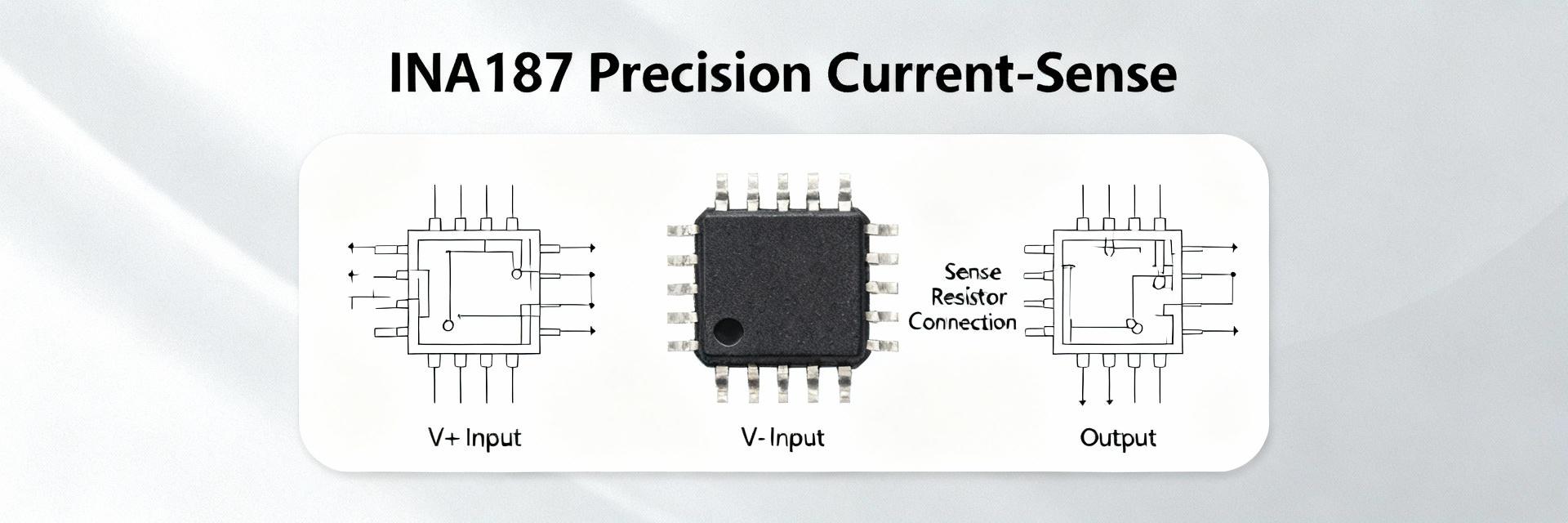
The INA187 is a bidirectional current‑sense amplifier optimized for high‑side and low‑side sensing where wide common‑mode range and precision matter. Key selling points include a wide common‑mode window, high input accuracy, and a bandwidth on the order of 650 kHz, which supports fast transient capture without complex front‑end filtering. Typical use cases are power monitoring and motor driver measurement where both polarity and speed of current changes are significant.
1.1 — Device overview & family positioning
Functionally, the INA187 amplifies the differential voltage across a shunt and presents a single‑ended output compatible with ADC inputs. It sits near the middle of its family: higher precision than economy parts, but lower complexity than op‑amp‑based front ends. Designers choose it when a modest bandwidth, tight offset, and broad common‑mode are required without adding external differential ADCs.
| Family | Typical CMR (V) | Common Gain Options |
|---|---|---|
| INA181/INA2181 (adjacent) | −0.2 to 36 | A = 1, 5 |
| INA187 | −2 to 42 | A = 1, 10 (example) |
| Higher BW variants | −2 to 42 | A = programmable |
1.2 — Typical application domains
Common application domains include high‑side sensing on battery rails, low‑side monitoring for thermal control, motor drive peak‑current measurement, and system power telemetry. Package options typically include small DFN/SOIC footprints for space‑constrained designs and automotive‑grade variants with extended temperature ranges for robust environmental operation.
2 — Key Electrical Specs Explained
Common‑mode voltage, supply limits, and survival ratings define where the amplifier can safely sense without distortion or latch‑up. The operational common‑mode range indicates guaranteed performance; survival limits indicate non‑destructive exposure. For design, always reserve conservative margins from the survival edges to account for transients and measurement error—this avoids temporary saturation or long recovery times during rail excursions.
2.1 — Common‑mode voltage, supply and survival limits
The stated operating common‑mode window of −2 V to +42 V means the amplifier maintains specified accuracy within that region. Survival to ±48 V implies the die remains undamaged outside the operating range but performance isn’t guaranteed. For example, on a 36 V automotive auxiliary rail, a 10% margin suggests designing for peak excursions under ≈39 V to preserve linearity and prevent output clipping during transients.
2.2 — Gain, bandwidth, slew rate, and stability considerations
Typical bandwidth near 650 kHz and a slew rate around 2.5 V/μs strike a balance between transient fidelity and noise. Higher gain increases output swing for small shunt voltages but narrows usable bandwidth; the designer must match gain to ADC sample rate and anti‑alias filtering. Rule of thumb: ensure amplifier bandwidth ≥ 5× ADC Nyquist frequency for faithful waveform capture, or add an RC to limit noise if sampling slowly.
3 — Noise, Accuracy, and Thermal Specs: What to Measure
Input‑referred noise, offset voltage, and gain error directly define smallest measurable current and long‑term stability. When measuring milliohm shunts, microvolt offsets translate to milliamps of error. Use the datasheet’s noise density and offset drift figures to estimate RMS error over your measurement bandwidth and to size the shunt for target resolution.
3.1 — Input‑referred noise, offset, and gain error
Input‑referred noise is specified in nV/√Hz; combine it with bandwidth to get RMS voltage noise. Example: if noise density is 12 nV/√Hz and bandwidth is 100 kHz, Vrms ≈ 12e‑9 * sqrt(1e5) ≈ 38 μV RMS. With a 10 mΩ shunt, that maps to ≈3.8 mA RMS uncertainty. Offset plus drift (tens of μV) further add a DC error term that must be considered for low‑frequency or DC current measurements.
| Shunt (mΩ) | Offset (μV) | Approx. Error (mA) |
|---|---|---|
| 10 | 50 | 5.0 |
| 5 | 50 | 10.0 |
| 1 | 50 | 50.0 |
3.2 — Power dissipation, junction temp, and thermal derating
Calculate shunt power (I^2R) and amplifier package dissipation (from quiescent current and output swing). Compare to θJA to estimate junction rise: ΔTj = Pd × θJA. If Pd = 0.2 W and θJA = 100 °C/W, junction rises 20 °C above ambient. Use thermal copper pours and vias to reduce θJA and derate gain/continuous measurement if ambient or enclosed temperatures approach maximum junction limits.
4 — How to Read the Datasheet for Design Decisions
A concise checklist turns datasheet numbers into actionable decisions: pick shunt for desired drop and power, choose amplifier gain to use ADC range, and design RC filtering to trade noise vs bandwidth. The goal is to maximize ADC dynamic range while keeping thermal and common‑mode margins in check; follow formulas and a worked example to validate choices before prototype PCB layout begins.
4.1 — Step‑by‑step checklist to pick shunt resistor, gain, and filter
Steps: (1) define Imax and target measurable resolution; (2) choose shunt: Vshunt_target = Imax × Rshunt (aim 20–50 mV for midrange ADC); (3) compute Rshunt = Vshunt_target / Imax and power Pd = Imax^2 × Rshunt; (4) choose gain so Vout = Gain × Vshunt fits ADC headroom. Worked example: Ipeak=100 A, target Vshunt=50 mV → R=0.5 mΩ, Pd_peak≈5 W, so use low‑value shunt with adequate thermal management and choose gain to place 50 mV near ADC full scale.
4.2 — PCB layout & decoupling best practices from datasheet guidance
Place shunt and amplifier input traces close and short, route differential inputs symmetrically, and keep analog ground reference near the amplifier return. Decouple supply pins with a 0.1 μF ceramic close to the device and a bulk cap nearby. Add Kelvin sense connections for the shunt and thermal reliefs beneath package copper to lower θJA; include test points for common‑mode and output monitoring and use differential scope probing techniques when verifying behavior under transients.
5 — Application Case Study + Troubleshooting
This case studies a motor‑drive current sensing implementation: specification required ±120 A peak measurement, 100 mA resolution, and operation off a 24–36 V rail. The chosen approach uses a low‑ohm shunt sized for 50–100 mV at peak, the INA187 at an appropriate gain to center output in ADC range, an RC filter to limit noise to below Nyquist, and copper pours for shunt cooling. Expected waveforms show bipolar pulses with fast edges captured within amplifier BW.
5.1 — Real‑world example: motor‑drive current sensing
Example calculations: target Vshunt at 120 A = 60 mV → Rshunt = 0.5 mΩ; continuous power at 50 A RMS ≈ 1.25 W, requiring a shunt rated >2 W. With Gain = 10, Vout_peak = 600 mV, ideal for a 3.3 V ADC with headroom. Add 1 kΩ || 100 pF RC at output to limit bandwidth for a chosen sample rate and to tame EMI from the motor drive.
5.2 — Common failure modes & how to debug with the datasheet
Common symptoms include output saturation during transients, offset drift with temperature, and unexpected noise spikes. Use the datasheet sections on common‑mode limits, supply transient immunity, and thermal ratings to map symptoms to causes: check common‑mode excursions against survival limits, verify decoupling and layout for supply dips, and measure ambient temperature vs computed junction temp to diagnose thermal drift.
Summary and Actionable Takeaways (Action recommendations)
- Verify common‑mode margin: ensure operating rail plus transients stay comfortably inside the −2 V to +42 V window to avoid nonlinear behavior or output saturation; reserve a safety margin for transients.
- Compute shunt and power: choose a shunt that produces a practical Vshunt at Imax (20–100 mV range), then confirm I^2R power and design PCB copper area to keep junction temperature within limits.
- Match gain and bandwidth to ADC: select amplifier gain to center the amplified shunt voltage in ADC range, and add RC filtering so that amplifier BW, noise, and ADC sampling align for the desired resolution and transient fidelity.
FAQ
H3: How does the INA187 handle large common‑mode voltages?
The INA187 supports an operating common‑mode from −2 V to +42 V and a survival rating to around ±48 V; this allows robust high‑side sensing up to typical 36 V rails. Designers should keep conservative margins from survival limits for transient events and follow datasheet guidance for supply decoupling and layout to prevent output distortion during excursions.
H3: What noise performance can I expect from the INA187 for shunt sensing?
Input‑referred noise is specified as a density (nV/√Hz); multiply by sqrt(BW) to get RMS voltage noise. For example, 12 nV/√Hz over 100 kHz yields about 38 μV RMS, which on a 10 mΩ shunt corresponds to roughly 3.8 mA RMS uncertainty. Use filtering to reduce bandwidth when high resolution is required.
H3: What layout and thermal measures are critical with the INA187?
Keep sense traces short and symmetric, use Kelvin connections for the shunt, place 0.1 μF decoupling capacitors close to supply pins, and add copper area/vias under the shunt and amplifier to lower θJA. Verify thermal rise with Pd × θJA and derate continuous current if ambient or enclosure temperatures are high to avoid offset drift and damage.








