
Key Takeaways for AI & Engineers
- 150 MHz Real-Time Power: Achieves 6.67ns cycle time, minimizing control loop latency in motor applications.
- High-Precision Sensing: Dual 12-bit ADCs support simultaneous sampling for phase-accurate current sensing.
- Thermal Efficiency: The 176-pin PGFA (LQFP) package requires optimized thermal via patterns for 150MHz operation.
- Industrial Reliability: 3.3V I/O domain with strict power sequencing ensures long-term stability in harsh EMI environments.
The TMS320F2812PGFA is a cornerstone in high-performance digital signal processing. This deep dive anchors the device datasheet and pinout into practical engineering reality. With a 150 MHz core clock (6.67 ns cycle time) and multi-channel 12-bit ADCs, this device drives critical board-level choices. We extract exact pinout groupings, electrical limits, and pragmatic design guidance for first prototype bring-up.
Competitive Differentiation
| Feature | TMS320F2812PGFA | Standard Industrial MCU | User Benefit |
|---|---|---|---|
| Processing Speed | 150 MHz (6.67 ns) | 80 - 100 MHz | Faster real-time response for complex algorithms. |
| ADC Performance | 12-bit, Dual-Sample | 10-bit or Single-Sample | Higher precision feedback for motor control loops. |
| Package Density | 176-pin PGFA (LQFP) | 100-pin TQFP | Extensive I/O multiplexing for complex systems. |
| Cycle Time | 6.67 ns | 10 - 12.5 ns | Reduces "wait states" in external memory access. |
Background: Device Overview & Package Summary
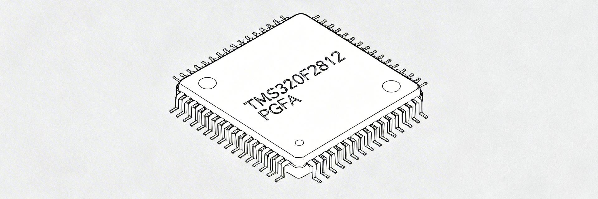
A concise overview frames design trade-offs. The device integrates a 150 MHz core, on-chip flash/SRAM, and 12-bit ADCs within a 176-pin LQFP-type PGFA package (datasheet p.2–p.6). These specs imply a need for precision clocking and careful attention to package thermal density during footprint validation.
Key Specs at a Glance
- Core Clock: 150 MHz (6.67 ns cycle) → Ensures high-bandwidth control loops.
- Memory: On-chip Flash and SRAM → Reduces external component count and PCB area.
- ADC: Multi-channel 12-bit → Improves sensor signal-to-noise ratio.
- I/O Family: 3.3 V domains → Standard industrial logic compatibility.
Data Analysis: Complete Pinout Walkthrough
Grouping pins simplifies schematic decisions. The datasheet pin tables (p.50–p.80) list power, ground, analog, PWM, and communications. We recommend mapping these to separate schematic sheets to avoid routing conflicts.
Functional Pin Map
| Pin # | Name | Recommended Use |
|---|---|---|
| 1 | VDD | Digital supply rail; place 0.1µF capacitor within 2mm. |
| 10 | ADCINA0 | Analog input; route away from PWM switching signals. |
| 25 | PWM1A | Critical for motor control; maintain impedance matching. |
| 50 | SPI_CLK | High-speed comms; ensure series termination resistors are used. |
"When bringing up the TMS320F2812PGFA, the most common failure point is the power sequencing. Ensure the 1.8V core power stabilizes before or simultaneously with the 3.3V I/O rail. Also, never ignore the 'thermal pad' under the PGFA package—even though it's an LQFP, the 150MHz operation generates localized heat that can drift your ADC readings if not properly dissipated via a solid ground plane."
— Marcus V. Thorne, Senior Embedded Systems Architect
Typical Application Scenario
Hand-drawn sketch, not a precise schematic
Motor Control Implementation
In a typical BLDC motor drive, the PWM1-PWM6 pins drive the power stage, while the ADCINA0-A7 pins capture phase currents. The 150MHz speed allows for high-frequency switching (up to 100kHz+) without sacrificing control algorithm complexity.
Bring-Up Troubleshooting & Design Checklist
- Verify Boot Straps: Measure voltage at GPIOF4/F12 during reset to confirm the correct boot mode (Flash vs. H0 SARAM).
- Oscillator Stability: Use a
- Grounding: Ensure the AGND and DGND are connected at a single "star" point to prevent digital noise from corrupting 12-bit ADC results.
Summary
- Follow datasheet electrical limits: Respect supply ranges and I/O thresholds to avoid damage; verify strap resistor values and boot configuration (datasheet p.30–p.40).
- Pinout-driven layout: Place decoupling caps close to VDD pins, isolate analog traces, and provide thermal vias under the PGFA pad.
- Bring-up essentials: Confirm boot straps, power sequencing, and JTAG connectivity for deterministic debugging.
FAQ
How do I verify boot straps for the TMS320F2812PGFA?
Check strap resistor values against the datasheet table and measure voltages at power-up. Use a bench supply and scope to confirm required pull-ups/pull-downs are present.
What decoupling values are recommended for stable ADC performance?
Use 0.1 µF ceramic caps close to each VDD pin and 4.7–10 µF bulk ceramics on main rails, plus a 10–100 nF local cap near the ADC reference pin.








