
The INA296B3EDRQ1 delivers gain error down to 0.1%, operates across a -5 V to 110 V common‑mode range, and consumes ~2.5 mA supply current — specs that place it among the most precise automotive‑grade current sense amplifiers available today. This brief uses those datasheet values as the baseline and focuses on practical limits, integration guidance, and reproducible test methods for power, automotive, and industrial engineers.
Targeted at system and test engineers designing high‑accuracy shunt measurement and protection systems, the document summarizes package and qualification details, dives into electrical performance and thermal behavior, and provides a hands‑on design checklist: PCB layout, input protection, calibration and production test recommendations. The primary takeaway: with correct layout, input protection, and calibration, the INA296B3EDRQ1 enables sub‑percent current measurements in high common‑mode environments without complex external circuitry.
1 — Background & Part Overview (Background introduction)
Package, Ordering & Device Variants
Point: The INA296B3EDRQ1 is supplied in an 8‑pin SOIC package and targets automotive applications with AEC‑Q100 qualification on the INA296x‑Q1 family. Evidence: device ordering codes map package, gain option and grade; TI lists multiple suffixes for gain and AEC versions. Explanation: the B3 suffix denotes the packaged variant with a grouped gain option; alternate INA296x family members provide different fixed gains and option codes for non‑automotive grades. Use the table below to map common suffixes to features and temperature grades.
| Suffix | Gain | Package | Qualification / Temp |
|---|---|---|---|
| B3 | Fixed gain (family dependent) | 8‑SOIC | AEC‑Q100 Grade 1 (−40 to 125/150°C operational range as specified) |
| B1 / B2 | Other fixed gains | SOIC / WSON | Commercial / Automotive options |
Functional Block & Typical Use Cases
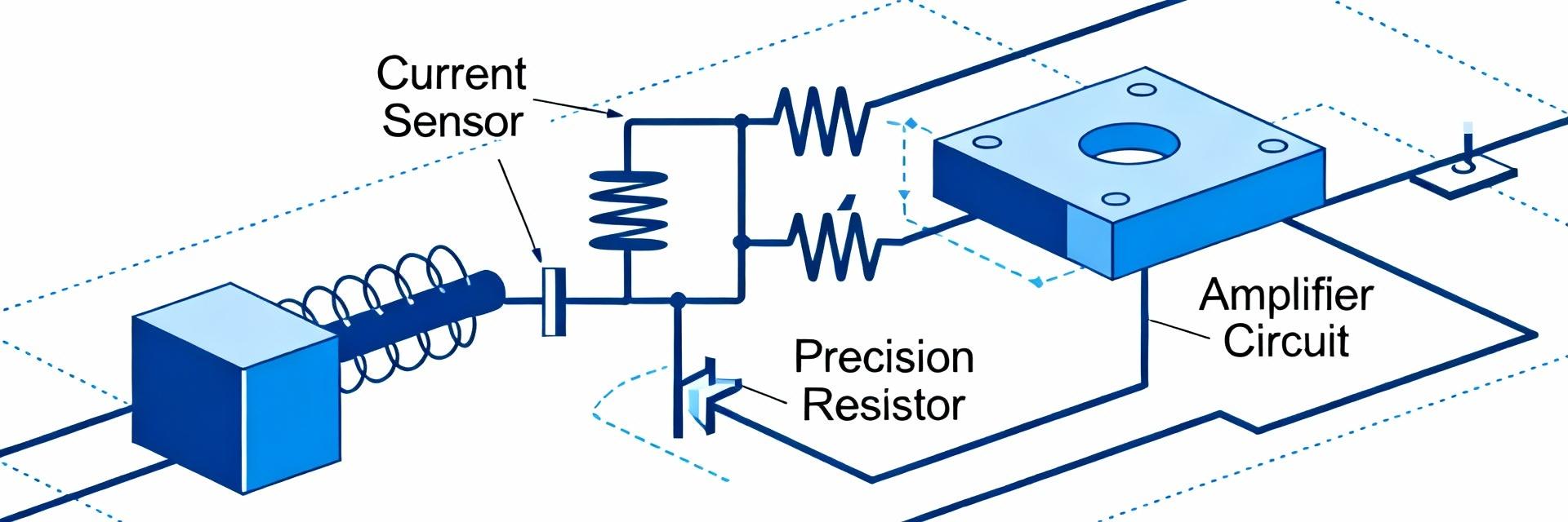
Point: Internally the device is a differential amplifier front end with integrated gain and bidirectional capability. Evidence: topology combines a precision input stage tolerant to high common‑mode voltages with a gain block and output stage optimized for single‑ended measurement. Explanation: that internal topology supports shunt‑based current measurement with minimal external components.
Typical use cases include shunt current measurement for power monitoring, battery management systems, motor control and inrush/current‑limiting detection. Recommendation: choose this device when you need high accuracy across high common‑mode voltages and prefer a minimal external component count; if you need higher bandwidth or lower noise, consider other INA296 variants with alternate gain/bandwidth tradeoffs.
Compliance & Automotive Qualification
Point: The INA296x‑Q1 family is designed to meet automotive reliability needs. Evidence: AEC‑Q100 qualification for the Q1 variants and extended junction temperature specifications are provided by the manufacturer. Explanation: this qualification impacts system‑level validation — qualifying a module that uses the device requires thermal cycling, HBM/ESD checks, and extended soak testing to ensure drift and offset remain within limits under automotive stressors.
Recommended qualification tests: thermal cycling across the operational range, power‑on/off and reverse‑voltage stress, and long‑term bias testing. For safety‑critical systems, run a design‑in qualification including sample‑level destructive analysis on first lots to confirm package robustness after reflow and mechanical stress.
2 — Key Electrical Specs & Real-World Performance (Data analysis)
Input / Common‑Mode Range & Overvoltage Behavior
Point: The stated common‑mode range is −5 V to 110 V and defines safe continuous operation. Evidence: near‑rail and transient behavior follows the datasheet tolerances; outputs may saturate near rails and recover with measurable clamps. Explanation: expect reduced linearity and increased output error when the input approaches the negative rail or exceeds the positive limit during transients.
Actionable transient test: apply a 1 kHz, 100 Vpp common‑mode step (rise time ~100 ns) with and without input protection; observe output clamp behavior and recovery time. Pass criteria: no latching, output returns to within specified offset limits within a few microseconds, and no hysteresis beyond datasheet listed overvoltage recovery. Include TVS clamps and series resistors if transients exceed the part’s rated handling.
Precision Metrics: Gain Error, Offset, Bandwidth, CMRR
Point: Typical gain error is 0.1%, input offset and drift are specified in the datasheet, bandwidth is ~1.1 MHz and slew rate ~8 V/µs for common INA296B variants. Evidence: these numbers enable AC and DC test planning. Explanation: gain error, offset, drift and CMRR determine achievable system accuracy and must be tested across temperature and common‑mode changes.
Actionable tests: DC gain test using four‑wire shunt measurement (apply known shunt current, measure output; tolerance ±0.2% for pass), swept‑sine for closed‑loop bandwidth (1 dB point within 1.1 MHz typical), and noise measurement using a low‑noise ADC or spectrum analyzer (define noise floor target per system SNR). For production, set pass/fail thresholds: gain error ≤0.5% (initial lot) and offset drift ≤ specified datasheet drift over intended temperature window.
Power & Thermal Performance
Point: Idle supply current ~2.5 mA yields predictable power dissipation (Pd = Vsup × Isupply). Evidence: at 5 V supply, Pd ≈ 12.5 mW; at 12 V supply, Pd ≈ 30 mW. Explanation: while die power is modest, thermal coupling in dense automotive PCB areas can raise junction temperature, affecting offset and drift.
Actionable thermal guidance: compute Pd and ensure adequate copper pours and thermal vias under and around SOIC pads. Example thermal calc: Pd = 12 V × 2.5 mA = 30 mW; with θJA ~ 100 °C/W (typical small SOIC on minimal copper), ΔT ≈ 3 °C — add copper pours and vias to reduce θJA if adjacent hot components exist. PCB layout guidance: implement at least one dedicated thermal island and several thermal vias under ground pad routes to distribute heat and minimize temperature gradients across the device.
3 — Design & Measurement Best Practices (Method guide)
PCB Layout & Routing for Accurate Current Sensing
Point: Layout dominates achieved accuracy more than component selection. Evidence: Kelvin sensing and minimized loop area reduce parasitic drops and common‑mode coupling. Explanation: following a checklist ensures repeatable performance across boards and lots.
- Place shunt close to the amplifier; minimize distance between shunt and Kelvin sense pins.
- Use short, wide Kelvin traces; avoid vias in the Kelvin path when possible.
- Create a ground island for amplifier reference and keep digital return currents away.
- Use guard traces around high‑impedance nodes and stitch with vias to internal ground planes.
Bad vs good layouts: bad — long sense traces running alongside switched power traces; good — isolated sense island, orthogonal routing of noisy signals, and dedicated ground stitching near the amplifier.
Input Protection & Filtering Strategies
Point: Transients and input capacitance can cause oscillation or damage. Evidence: series resistors and RC filters tame input bandwidth and limit surge current into input structures. Explanation: balance between protection and measurement bandwidth is key for systems up to 100s of kHz.
Actionable ranges: TVS clamp voltages selected just above 110 V common‑mode rating for high‑voltage rails; series resistors 10–100 Ω to limit surge currents and isolate input capacitance; input RC time constants targeting 1/(2πRC) around 100 kHz for 100 kHz systems and up to 1 MHz for higher bandwidths — e.g., R=33 Ω, C=47 pF yields fc≈103 kHz. Ensure RC damping does not create significant gain error at your measurement bandwidth.
Test Fixtures & Measurement Setup
Point: Reproducible fixtures and measurement hygiene are mandatory for accurate characterization. Evidence: four‑wire shunt setups and proper probe grounding reduce measurement artifacts. Explanation: poor probing can mask device performance and falsely indicate failures.
- Use four‑wire shunt for DC accuracy tests; Kelvin leads directly to measurement instrument.
- For dynamic tests, use a differential active probe and keep probe ground leads minimal.
- Capture step response, bandwidth sweeps, and common‑mode transient recovery on a 100 MHz+ scope with adequate sampling.
Expected oscilloscope captures: step response (rise time and overshoot ±), common‑mode transient capture demonstrating clamping and recovery, and swept sine overlay showing 1 dB bandwidth. Pass criteria should be defined per system accuracy targets (e.g., step overshoot
4 — Comparative Analysis & Application Case Studies (Case showcase)
Head‑to‑Head: INA296B3EDRQ1 vs. Comparable Parts
Point: Tradeoffs across accuracy, bandwidth, input range and cost determine part selection. Evidence: INA296 family offers variants with distinct gain/bandwidth that compete with similar automotive current sense amplifiers from other vendors. Explanation: use the compact table below to guide selection based on target metrics.
| Metric | INA296B3EDRQ1 | Other INA296 variants / competitors |
|---|---|---|
| Gain error (typical) | 0.1% | 0.1–0.5% |
| Bandwidth | ~1.1 MHz | 0.5–5 MHz (variant dependent) |
| CM range | -5 V to 110 V | Similar or higher for specialized parts |
| Automotive grade | Q1 available | Varies |
| Cost | Moderate | Varies |
Selection guidance: prioritize INA296B3EDRQ1 when automotive qualification and high accuracy across wide common‑mode are primary; choose higher‑bandwidth variants when dynamic fidelity is the key requirement, accepting potential tradeoffs in noise or cost.
Real‑World Application Examples
Case 1 — High‑side battery management: configure for gain to map max expected battery current to ADC full scale; recommended shunt 50–100 µΩ for high‑current EV subsystems, input RC to filter switching noise but preserve transient detection, and two‑point calibration to remove offset at zero current.
Case 2 — Motor current sensing: use mid‑range shunt and pair with a fast RC (fc near 200–300 kHz) to capture commutation events while attenuating switching spikes; ensure layout keeps high switching return currents away from sense nodes and use TVS protection for inverter transients.
Failure Modes & Troubleshooting Checklist
Point: Common problems include thermal offset drift, oscillation from input capacitance, and false readings due to ground loops. Evidence: these failure modes recur in production debug unless layout and protection are addressed. Explanation: follow a methodical debug flow to isolate the root cause.
- Reproduce: capture failing condition with differential probe and log supply/common‑mode.
- Isolate: swap suspect board sections, test with short Kelvin leads and remove input filters to see if oscillation persists.
- Measure: quantify offset vs. temperature and common‑mode using a thermal chamber and precision current source.
- Fix: apply RC damping, increase series resistance, add guard traces, or move sensitive traces away from noisy returns.
5 — Integration Checklist & Deployment Recommendations (Action suggestions)
BOM & Manufacturing Considerations
Point: Component choices and assembly influence performance and yield. Evidence: shunt tolerances and decoupling placement change system accuracy. Explanation: keep BOM minimal but spec critical parts tightly.
| Component | Recommendation |
|---|---|
| Shunt resistor | Low TCR |
| TVS | Clamp just above 110 V; power rating per expected surge energy |
| Bypass caps | 0.1 µF + 10 µF near supply pins, low ESL types |
Assembly notes: pay attention to ESD handling and reflow profiles recommended in package addendum; avoid excessive preheat to maintain AEC margins.
Calibration, Firmware & Signal Conditioning
Point: System calibration removes residual offset and gain error; firmware filtering improves SNR. Evidence: two‑point calibration compensates for shunt tolerance and amplifier offset. Explanation: combine hardware and firmware to meet long‑term accuracy targets.
Pseudo‑code for two‑point calibration:
1. Measure Vout at I=0 → offset
2. Measure Vout at I=Iref → slope
3. Gain_cal = (Iref) / (Vout_Iref - offset)
4. Apply digital correction: I_meas = Gain_cal * (Vout - offset)
Suggested digital filter cutoffs: set cutoff at 1/3 to 1/10 of sampling Nyquist depending on dynamic needs — e.g., for 10 kSPS sample rate, lowpass at 1–3 kHz.
Production Test & Qualification Plan
Point: A lean production test matrix catches early defects without excessive cycle time. Evidence: DC gain/offset checks, spot noise measurements and thermal soak provide high coverage. Explanation: define thresholds and sample sizes for early runs, tighten as yield stabilizes.
- DC gain/offset: measure at 0 A and Iref; pass if gain within ±0.5% and offset within specified mV.
- Noise spot check: measure RMS noise at defined bandwidth; fail if above target.
- Thermal soak: sample units subjected to 85°C for 2 hours; monitor offset drift.
Summary
The INA296B3EDRQ1 is an ultra‑precise, automotive‑grade current sense amplifier suited for high‑accuracy, high common‑mode applications. With correct PCB layout, robust input protection and an effective calibration flow, systems can reliably achieve sub‑percent measurement accuracy across harsh environments. Practical deployment centers on three action points: attention to layout and Kelvin sensing, adequate transient protection with carefully chosen RC damping, and a reproducible calibration and production test plan.
- Layout: place shunt and amplifier close together, use short Kelvin traces and a dedicated ground island to minimize parasitics and common‑mode coupling for accurate INA296B3EDRQ1 readings.
- Input protection: combine TVS clamps and series resistors plus tuned RC filters (example R=33 Ω, C=47 pF) to protect against transients while preserving required bandwidth.
- Calibration: implement two‑point digital calibration and set digital filter cutoffs at 1/3–1/10 of Nyquist to balance noise rejection and dynamic response for the current sense amplifier subsystem.
FAQ
How do I test INA296B3EDRQ1 gain error and offset?
Use a four‑wire shunt and precision current source. Measure Vout at I=0 for offset, then at a known reference current Iref; compute gain as Iref/(Vout_Iref − Vout_0). Run over temperature to capture drift. Pass/fail thresholds typically set at gain error ≤0.5% and offset within datasheet limits for initial production; tighten thresholds as confidence grows.
What input protection is recommended for a high‑voltage current sense amplifier application?
Recommend a TVS sized for transient energy with a clamp above the continuous 110 V rating, series input resistors (10–100 Ω) to limit surge currents, and RC filtering sized for your bandwidth (e.g., R=33 Ω, C=47 pF for ≈100 kHz). Ensure protection elements do not create excessive voltage drop affecting measurement accuracy.
Which PCB layout practices ensure best accuracy with the INA296B3EDRQ1?
Keep Kelvin sense traces short and wide, isolate the amplifier reference with a small ground island, avoid routing noisy switcher returns near sense traces, and add guard traces and thermal vias. Place decoupling caps close to supply pins and use a separate plane or island for high‑current paths to prevent ground‑bounce induced errors.








