
🚀 Key Takeaways: SN74LVC1G125DCKR Insights
- Universal Logic: Operates from 1.65V to 5.5V, enabling seamless interfacing between legacy 5V and modern 1.8V rails.
- Safe Hot-Swapping: Integrated Ioff circuitry prevents current backflow, protecting unpowered sub-systems.
- High-Speed Drive: Delivers up to 32mA output current, ensuring signal integrity across high-capacitance bus lines.
- Ultra-Compact: The SC70-5 (DCK) package reduces PCB footprint by ~40% compared to standard SOT-23 buffers.
The SN74LVC1G125DCKR is introduced here as a compact single buffer with a three‑state output optimized for low‑voltage systems. The device supports a wide supply range from 1.65 V to 5.5 V and offers strong output drive capability, making it suited for level translation, bus isolation, and IO buffering in space‑constrained designs. This article distills the datasheet into actionable guidance for selection, schematic capture, layout, and validation.
Translates to: Reliable signal transmission over longer PCB traces without significant voltage drop.
Translates to: Zero leakage when Vcc=0V, extending battery life in modular/portable electronics.
Evidence from the official datasheet shows the part includes Ioff for partial power‑down support, a true three‑state output, and significant IO drive capability up to roughly 32 mA under specified conditions. The following sections translate those headline specifications into pinout mapping, electrical cautions, timing budgeting, layout best practices, test procedures, and an integration checklist to speed design and reduce iteration.
1 — Quick Overview & What the Datasheet Reveals (Background)
Purpose & typical applications
Point: The device is a single 3‑state buffer used to control data flow on shared nets. Evidence: The datasheet classifies it as a single buffer with a three‑state output and Ioff support. Explanation: Typical uses include bus buffering, level‑shifting protection when one side may be powered down, partial power‑down isolation on shared buses, and providing higher drive for IO lines that must source or sink tens of milliamps during bus arbitration.
Key datasheet highlights at a glance
Point: Engineers need a compact summary for quick decision making. Evidence: Key electrical ranges and behaviors are specified in the datasheet tables. Explanation: The table below captures the headline specs designers repeatedly check when selecting this device.
| Parameter | SN74LVC1G125DCKR (This Model) | Competitor (Standard 74AHC Series) |
|---|---|---|
| Voltage Range | 1.65V to 5.5V (Ultra-wide) | 2.0V to 5.5V (Limited) |
| Output Drive (Iol) | ±32 mA (High Drive) | ±8 mA (Standard) |
| Power-Down (Ioff) | Supported (Isolation ready) | Rarely Supported |
| Package Area | ~4.2 mm² (SC70-5) | ~8.4 mm² (SOT-23-5) |
2 — SN74LVC1G125DCKR Pinout & Package Details (Data / Pinout)
Pin assignment and functions
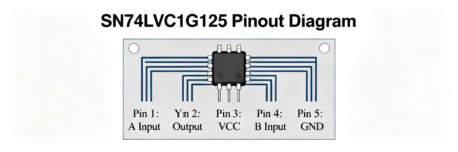
Point: Understand pin roles before schematic and layout. Evidence: The package has labelled pins for input, output, enable, ground, and VCC. Explanation: Pin names are A (input), OE (output enable control), Y (output), VCC (power) and GND (ground). OE is a control input that asserts the device output to either drive the line or enter high‑impedance; consult the symbol and truth table in the datasheet to confirm active polarity during capture.
🛡️ Engineer's Field Notes & Pro Tips
"During high-speed switching, the SC70 package can exhibit ground bounce if decoupling isn't immediate. Always place your 100nF cap within 2mm of Pin 5 (VCC)." — Marcus V. (Senior Hardware Architect)
- Selection Pitfall: Don't confuse with the 'G126' variant. The 'G125' has an Active-Low Output Enable (OE).
- Thermal Tip: While small, driving 32mA continuously at 5.5V generates localized heat. Ensure ground pins connect to a solid plane for heat sinking.
Package options, footprint and mechanical notes
Point: Package choice impacts footprint and assembly. Evidence: The device is offered in a small five‑lead package optimized for tight board real estate. Explanation: The DCK (SC70‑5) small outline reduces BOM area; follow the mechanical drawing for pad dimensions and solder mask openings. For reflow, use standard lead‑free profiles and follow recommended stencil aperture ratios; if an exposed pad is not present, thermal relief is achieved through copper pours and vias on the ground plane.
3 — Electrical Characteristics & Absolute Maximums (Data Analysis)
Figure 1: Typical logic level isolation scenario using the OE pin.
DC electrical characteristics to watch
Point: Key DC specs determine compatibility in mixed‑voltage systems. Evidence: The datasheet specifies VCC limits, input thresholds, static input leakage, output drive characteristics, and Ioff behavior. Explanation: VCC must be maintained between the stated minimum and maximum; VIH/VIL thresholds scale with VCC so margins tighten at lower supplies. Account for static input leakage and Ioff when multiple rails coexist; design pull‑ups/pull‑downs to hold lines in known states when OE is inactive or when parts are powered down.
Absolute maximum ratings and safe‑operating areas
Point: Violating absolute maximums damages devices. Evidence: The datasheet lists absolute ratings such as maximum VCC, input voltage excursions relative to VCC, and ESD classes. Explanation: Avoid driving inputs beyond the device VCC or beyond the specified input swing; if inputs could exceed VCC, add level protection or series resistors. Use derating: keep operating stresses well below absolute limits and allow margin for transient events and hot‑plug conditions.
4 — Timing, Performance & Signal Integrity (Data Analysis)
Propagation delay, output enable/disable timing and drive capability
Point: Timing specs determine bus arbitration windows. Evidence: The datasheet gives propagation delays (A→Y) and enable/disable times for OE transitions under defined load and VCC conditions. Explanation: Budget tPD and tPZ/tPLZ when sequencing multiple devices on a bus; slower enable/disable transitions increase the risk of contention. Include device timing in worst‑case timing diagrams and add margins for process, temperature, and VCC variation.
Timing diagram (conceptual):
  A -----+       _____
         |------+     \____ Y (driven after tPD)
  OE ---\_/----+        \_  (OE disable -> high‑Z after tPZ)
Signal integrity and layout best practices
Point: Layout affects rise/fall times and bus stability. Evidence: Datasheet loads and capacitance specs indicate sensitivity to capacitive loading. Explanation: Use a 0.1 µF ceramic decoupling capacitor placed within 2.5 mm of the VCC pin, add a 1 µF bulk nearby, and consider series resistors (22–47 Ω) on outputs to dampen ringing when driving capacitive traces. Keep OE traces short to minimize skew and avoid driving long stubs on shared buses.
5 — Design Integration: Schematics, Typical Circuits & PCB Tips (Method / How‑to)
Typical circuit examples
Point: Three common integration patterns speed adoption. Evidence: Datasheet features like Ioff and enable control enable these patterns. Explanation: (1) Level‑translate one IO between 1.8 V and 3.3 V by powering the device from the target domain and using pull resistors (10 kΩ) where needed; (2) Bus isolation with OE tied to an MCU pin and a pull‑down or pull‑up to define the idle state; (3) Partial power‑down: rely on Ioff so an unpowered node does not backfeed the active rail—verify with bench tests and add series resistors if uncertain.
PCB placement, decoupling and thermal considerations
Point: Placement and decoupling reduce noise and improve reliability. Evidence: Recommended decoupling placement in the datasheet and typical assembly guidance. Explanation: Place the 0.1 µF decoupling capacitor adjacent to the VCC pin within ~0.1 inch, route VCC and GND with short, wide traces, keep OE routing short relative to the fastest timing nets, and avoid analog signal routing beneath the package. For thermal management, use copper pours and thermal vias if power dissipation is expected to rise due to high switching activity.
6 — Validation Checklist, Troubleshooting & Test Procedures (Action)
✅ Pre-Production Checklist
- Verify OE pin polarity (Logic LOW = Output Enabled).
- Confirm VCC is within 1.65V – 5.5V for all power profiles.
- Check that input voltages never exceed 5.5V regardless of VCC.
- Verify decoupling cap placement (
Common failure modes and fixes
Point: Typical problems have straightforward remedies. Evidence: Symptoms often map to layout, power sequencing, or pin errors indicated in datasheet warnings. Explanation: Incorrect pin mapping yields nonfunctional nets—double‑check silkscreen and footprint; bus contention can be remedied with proper OE sequencing or added series resistors; missing decoupling causes noise—add caps near VCC; ESD damage requires replacement and ESD handling improvements during assembly.
Summary
The SN74LVC1G125DCKR is a compact single 3‑state buffer whose datasheet‑stated features (1.65–5.5 V operation, three‑state output, Ioff support and substantial output drive) make it a strong candidate for mixed‑voltage buffering and bus isolation. Use the pinout, timing, and layout guidance above to finalize footprint, timing budgets, and validation steps before production to avoid common integration pitfalls.
- Use the device for level translation and bus isolation; confirm supply selection within 1.65–5.5 V and validate Ioff behavior during power sequencing to prevent back‑feeding.
- Place a 0.1 µF decoupler within 2.5 mm of VCC, add a 1 µF bulk nearby, and keep OE traces short to protect timing margins and reduce contention risk.
- Budget propagation and enable/disable delays in system timing diagrams; add small series resistors on long or capacitive traces to control ringing and reduce EMI.








