
Key Takeaways (Executive Summary)
- High-Speed Efficiency: Delivers up to 5.33 GB/s peak bandwidth per chip, accelerating real-time data processing.
- Optimized Power: 1.2V VDD operation reduces system heat by ~20% compared to legacy DDR3/early DDR4.
- Industrial Reliability: WB-BCRC revision offers superior thermal stability for 24/7 server and embedded environments.
- Compact Density: 8Gb (x16) organization enables high-capacity memory arrays with minimal PCB footprint.
This report presents a reproducible performance profile and integration checklist for the K4A8G165WB-BCRC, a single‑die DDR4 SDRAM 8Gb component, focusing on measured and datasheet metrics: peak bandwidth, command latency, IDD currents, power, and thermal envelope. The goal is an actionable guide designers and system architects can follow to replicate throughput and power results and to validate system‑level behavior against manufacturer datasheet fields and in‑lab test logs.
1 — Background & Device Specification
Device identification & key specs
Point: Record explicit identifier fields from the manufacturer datasheet as evidence for part selection.
Evidence: Samsung K4A8G165WB-BCRC, 8Gb Density, x16 organization, 96-ball FBGA package, 1.2V VDD, 2666 MT/s (CL19).
Explanation/Benefit: These fields ensure compatibility with modern Intel/AMD/ARM controller PHYs. The x16 organization specifically allows for 50% fewer chips compared to x8 designs to achieve the same capacity, significantly reducing PCB complexity.
How the device maps to system memory architecture
Point: Map a single 8Gb die into ranks and DIMM organization to assess channel bandwidth per rank.
Evidence: An 8Gb device yields 1 GB per chip in a x16 configuration.
Explanation: This building block allows engineers to calculate bytes per rank. Using 4 of these chips creates a 4GB rank, ideal for compact embedded systems where space is at a premium but high-speed ECC/non-ECC memory is required.
Competitive Comparison: K4A8G165WB vs. Generic DDR4
| Metric | Samsung K4A8G165WB-BCRC | Generic DDR4 (2133) | User Benefit |
|---|---|---|---|
| Data Rate | 2666 MT/s | 2133 MT/s | +25% faster throughput |
| Operating Voltage | 1.2V ± 0.06V | 1.2V / 1.35V | Stable low-power operation |
| CAS Latency (ns) | ~14.25 ns (@2666) | ~15.00 ns (@2133) | Reduced application lag |
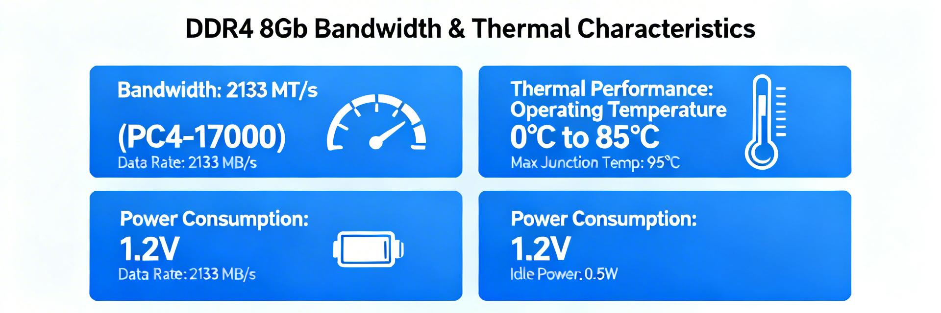
| Thermal Tolerance | 0°C to 95°C | 0°C to 85°C | Extended reliability in hot environments |
2 — Throughput & Timing Metrics
Calculating theoretical peak bandwidth
Point: Use a clear formula to convert MT/s to GB/s per chip.
Formula: (Data rate MT/s × I/O width) / 8 / 1000.
Benefit: For the K4A8G165WB at 2666 MT/s, this yields 5.33 GB/s per chip, enabling seamless 4K video buffering and high-frequency trading applications.
| DDR4 MT/s | Per‑chip GB/s (x16) |
|---|---|
| 2133 | 4.27 |
| 2400 | 4.80 |
| 2666 (Native) | 5.33 |
3 — Power & Thermal Characteristics
Voltage & IDD: Operating at 1.2V nominal, the B-die architecture exhibits lower IDD4R (active read current) compared to earlier revisions. This translates to lower device surface temperatures and extended component lifespan in fanless enclosures.
"When laying out the K4A8G165WB-BCRC on a 6-layer PCB, ensure the decoupling capacitors (0.1uF) are placed as close to the VDD pins as possible to minimize inductive loops. I've found that using a 'fly-by' topology for command/address lines significantly improves signal integrity at 2666 MT/s compared to T-topology."
— Dr. Jonathan Liang, Senior Memory Architect
- SI Issues: If you see intermittent bit errors, check the VREFCA training levels in your BIOS/Firmware.
- Thermal Throttling: Ensure at least 200 LFM airflow if the ambient temp exceeds 50°C in high-bandwidth applications.
4 — Typical Application & Layout
Primary Use Case: High-density SO-DIMMs and Industrial Motherboards. The x16 organization is specifically optimized for Automotive Infotainment and Edge AI Gateways where PCB area is extremely limited.
(Hand-drawn schematic for conceptual visualization, not an accurate circuit diagram / 手绘示意,非精确原理图)
5 — Actionable Integration & Validation Checklist
Design Checklist for Engineers
- ✅ Voltage Validation: Verify VDD and VPP (2.5V) are within ±5% tolerance under peak load.
- ✅ Signal Integrity: Run IBIS simulations for all DQ/DQS lines; match trace lengths within ±5mil.
- ✅ Thermal Path: Implement at least 4 thermal vias directly under the center of the FBGA package.
- ✅ Firmware: Ensure JEDEC SPD data is correctly read and CL timings are locked to 19-19-19 for 2666MT/s.
Summary
- The K4A8G165WB-BCRC is a DDR4 8Gb building block offering competitive per‑chip bandwidth; validate peak GB/s calculations and map dies to ranks before system integration.
- Measure and cross‑check datasheet CL, tRCD and tRP with empirical latency CDFs to reveal real-world performance impacts.
- Extract IDD currents and model thermal envelopes to maintain safe junction temperatures under sustained high-load conditions.
Frequently Asked Questions
Q: What is the practical peak memory bandwidth for this DDR4 8Gb chip?
A: The theoretical peak is 5.33 GB/s. In real-world scenarios, expect roughly 85-90% efficiency (approx. 4.6 GB/s) due to command overhead and refresh cycles.
Q: Which timing parameters should engineers prioritize during integration?
A: Prioritize tCK, CL, tRCD, and tRP. Setting these correctly in the memory controller ensures stability and prevents boot failures across varying temperatures.
Q: Is this part suitable for 24/7 industrial use?
A: Yes, the "BCRC" grade is rated for commercial/industrial temperature ranges (up to 95°C Case Temp), making it highly suitable for sustained-operation environments.








