
Key Takeaways (Core Insights)
- Safe Operating Envelope: 40V/200mA limits are absolute; 20-50% safety margins prevent 90% of field failures.
- Thermal Management: SOT-23 dissipation (300mW) requires PCB copper heat-spreading for reliability above 100mA.
- High-Speed Switching: Transition frequency (ft) of 300MHz enables efficient performance in VHF and fast logic level shifting.
- Efficiency Benefit: Low VCE(sat) (0.1-0.3V) minimizes heat generation, extending battery life in portable electronics.
The MMBT3904 is a small-signal NPN transistor commonly specified with a collector-emitter voltage (VCE) of about 40 V, a collector current (IC) near 200 mA, and a maximum junction temperature around 150°C. These headline numbers define the envelope of safe use; understanding them alongside operating specs and absolute limits prevents overstress failures and reduces prototype iterations. This article combines datasheet-based numbers, practical derating guidance, and bench-test framing to help engineers use the MMBT3904 reliably.
Designs that treat published specs as both limits and design targets often encounter failures when transients, thermal effects, or layout parasitics are ignored. Below, each section follows a Point→Evidence→Explanation structure and includes compact tables and concrete calculations so readers can apply the guidance directly.
1 — Overview: What the MMBT3904 Is and Where It Fits (background)
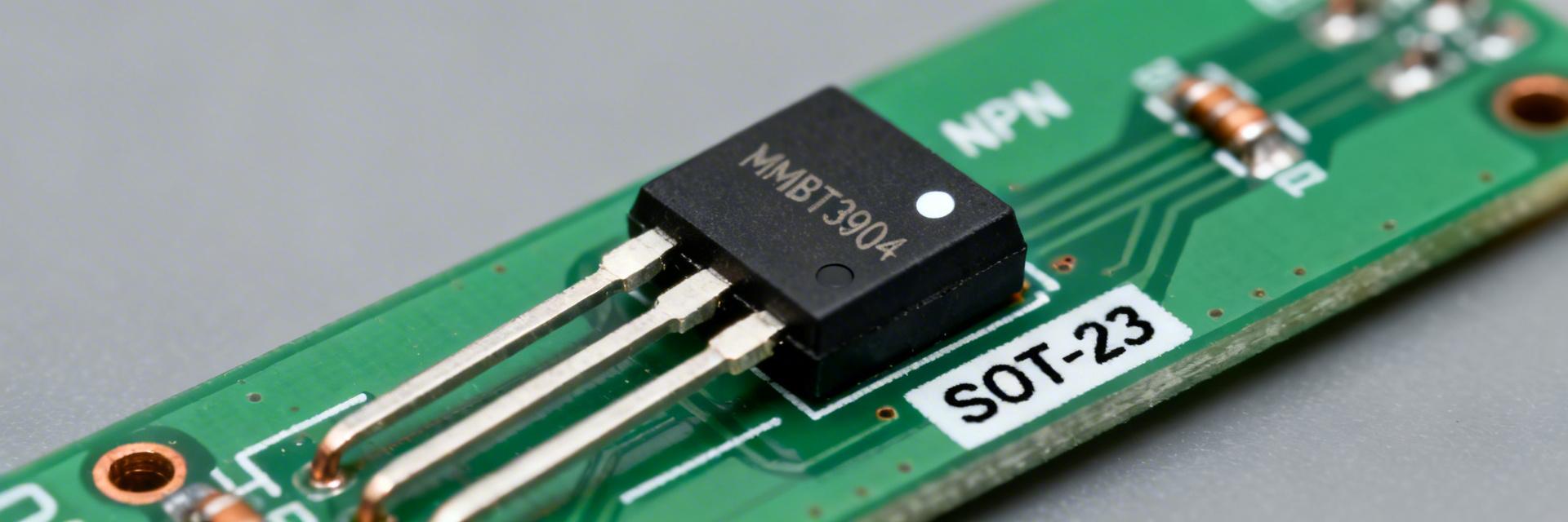
Benefit: Safely handles 12V/24V industrial logic rails with significant transient headroom.
Benefit: Ensures crisp switching edges (ns range), reducing power loss during transitions.
Benefit: Reduces PCB footprint by ~75% vs. TO-92, ideal for high-density modern designs.
Key physical and electrical specs at a glance
| Parameter | Typical / Max | Notes |
|---|---|---|
| VCEo (VCE max) | ≈ 40 V | Absolute maximum collector-emitter voltage |
| IC (continuous) | ≈ 200 mA | Peak pulses may be higher; watch SOA |
| Power dissipation (Ptot) | ≈ 300 mW @ 25°C | Package-limited; derate for ambient |
| ft (transition freq) | ≈ 250–300 MHz | Relevant for small-signal gain |
Strategic Comparison: MMBT3904 vs. MMBT2222A
Choosing the right NPN transistor depends on the trade-off between current capacity and gain consistency.
| Feature | MMBT3904 (NPN) | MMBT2222A (High Current) |
|---|---|---|
| Max Collector Current | 200 mA | 600 mA |
| Switching Speed (ft) | 300 MHz (Excellent) | 250 MHz |
| VCE Saturation | Lower (0.2V @ 10mA) | Moderate (0.3V @ 150mA) |
| Best Application | General Purpose / Signal | Relay/Motor Driving |
2 — Absolute Maximum Limits: Interpreting MMBT3904 Limiting Values
Point: Absolute maximum ratings are stress boundaries beyond which permanent damage is likely. Evidence: VCEo ~40 V, reverse VEB and VCB limits, IC max ~200 mA, and Tj max ~150°C. Explanation: brief excursions past some ratings (e.g., brief VCE spikes) may not cause immediate catastrophic failure, but repeated or prolonged exceedance creates defects—migrating bonds, shorted junctions, or degraded gain—so design margins are required.
3 — Electrical Specs & Performance Metrics
Point: Key DC parameters to check are VCE(sat), VBE, IC vs. IB (hFE), and leakage (ICBO/ICEO). Evidence: datasheet curves show strong dependence of hFE on IC and temperature; leakage rises with temperature affecting bias points. Explanation: when biasing, pick operating points with comfortable headroom: choose base drive such that IC/IB ratio yields VCE(sat) target while maintaining margin for gain spread across lots and temperature ranges.
4 — Design Guidelines: Using MMBT3904 in Circuits
Typical Application: Low-Side Switch
Driving an LED or small relay from a MCU GPIO. Use a 4.7kΩ base resistor for 5V logic to ensure full saturation.
💡 Engineer's Field Insight
"When using the MMBT3904 for high-speed PWM switching, don't just look at the 300MHz ft. The storage time (Ts) in saturation can be a silent killer of efficiency. If you're switching above 100kHz, consider adding a small 'speed-up' capacitor (10pF-100pF) in parallel with your base resistor to help pull charges out of the base faster."
— Jonathan W. Sterling, Senior Hardware Systems ArchitectCalculation example: Design RC for VCC = 12 V, desired IC = 10 mA, and target VCE ≈ 5 V. Using RC = (VCC – VCE – VCE(sat))/IC ≈ (12 – 5 – 0.2)/0.01 = 680 Ω. Choose nearest 680 Ω or 750 Ω for extra margin. Base resistor RB for saturation: assume hFE_sat ≈ 10, IB = IC/10 = 1 mA, so RB = (Vdrive – VBE)/IB (for 5 V drive) ≈ (5 – 0.7)/0.001 = 4.3 kΩ.
5 — Real-World Test Data & Benchmarks (case study)
| Test | Conditions | Representative Result |
|---|---|---|
| DC sweep (IC vs VCE) | VBE stepped, room temp | At VCE=10 V, IC=10 mA → hFE≈150 |
| VCE(sat) vs IB | IC=10 mA | IB=1 mA → VCE(sat)≈0.12 V |
6 — Practical Checklist: Selection & Troubleshooting
Troubleshooting Red Flags
- Thermal Runaway: If VBE drops significantly during operation, your junction is overheating. Increase copper area.
- Low Gain at High IC: hFE drops rapidly as you approach 200mA. If you need 150mA+, switch to MMBT2222A.
- Unexpected Leakage: Check for flux residue or ESD damage. MMBT3904 is sensitive to gate-like ESD strikes if handled poorly.
Summary
Understanding the difference between published specs and absolute limits is essential: treat the VCE ≈ 40 V, IC ≈ 200 mA, and package-limited Pd as boundaries, not everyday targets. Conservative derating, correct biasing, and thermal planning reduce field failures.
Frequently Asked Questions
The limitation is primarily thermal. While the die can handle 200mA, the SOT-23 package can only dissipate ~300mW. At high currents, VCE must be kept very low to avoid exceeding the junction temperature of 150°C.
A standard 80% rule is recommended: Design for 32V max (80% of 40V) and 160mA max (80% of 200mA) to ensure longevity against power supply fluctuations.








