
Point: In space-constrained electronics, compact board-to-wire housings are a common choice for dense signal routing. Evidence: The 1.00mm pitch, 20-pin form factor balances PCB area savings and routing complexity, where designers routinely trade area for tighter trace/annular requirements. Explanation: This guide breaks the part into verifiable specs, practical layout rules, comparison data, and a validation checklist to reduce integration risk.
Point: Engineers need concise, testable guidance when selecting a miniature housing. Evidence: Typical use cases include sensor arrays, camera/display links, and internal harnesses with low-current signals. Explanation: The following sections cover why designers choose this class of connector, electrical/mechanical limits, selection heuristics, and layout best practices.
Background & Common Applications
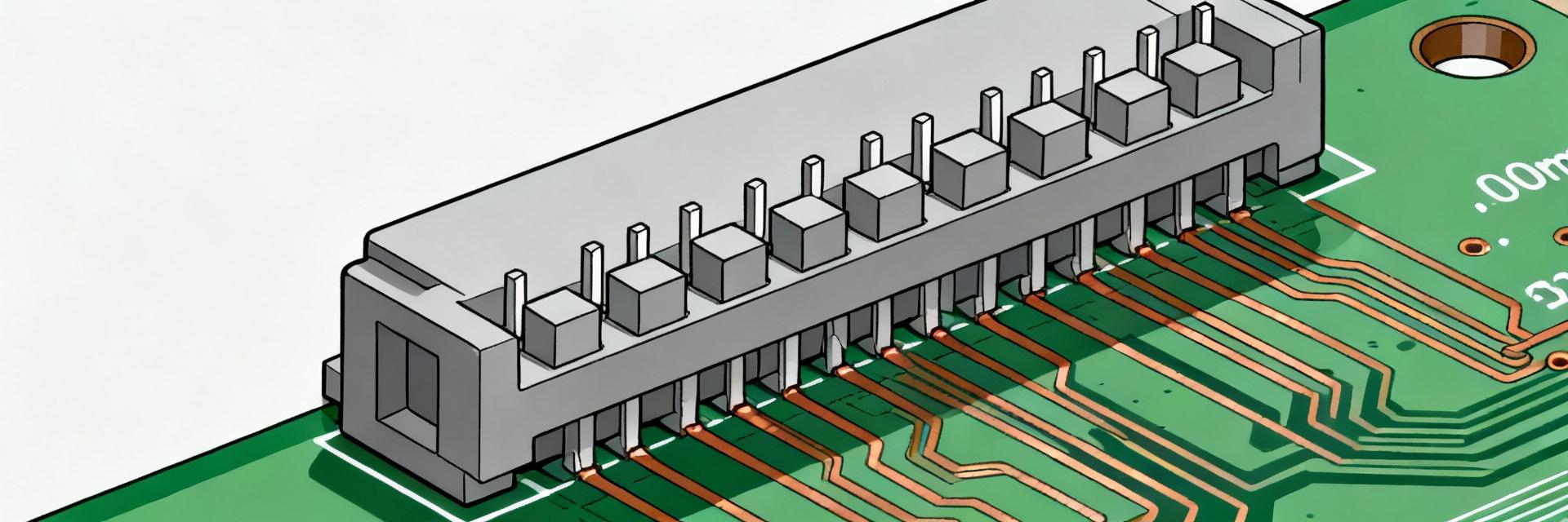
Why Designers Pick 1.00mm Pitch
Point: Density vs. manufacturability drives the choice.
Evidence: 1.00mm pitch typically reduces footprint by 25–40% compared to larger pitches while increasing solder bridge risk.
Explanation: For low-current digital buses (I2C, UART, GPIO), space savings justify tighter process control and AOI investment.
Typical Application Verticals
Point: Common in compact modules and internal harnesses.
Evidence: Found in sensor modules, handhelds, and thin displays.
Explanation: Mating retention and polarization are vital in vibration-prone contexts to ensure long-term reliability.
Key Specifications & Mechanical Dimensions
Electrical & Thermal Limits
Point: Verify ratings against system needs.
Evidence: 0.8–1.5 A per contact, 30–50 V rating, and -40 to +105 °C range.
Explanation: Apply derating for bundled wires and validate with thermal cycling tests at expected currents.
Mechanical & Footprint Guidance
Point: Confirm core dimensions before PCB release.
Evidence: A 20-position housing measures ~11–12 mm in length with defined keepout zones.
Explanation: Follow vendor recommendations for pad length and reserve clearance for mating latches.
Comparative Data & Selection Criteria
Choosing the right pitch is a balance between board real estate and assembly robustness.
| Pitch | Contact Count | Typical Current | Min Board Area | Assembly Class |
|---|---|---|---|---|
| 0.8 mm | 8–80 |
0.5–1.0 A
|
Smallest | Fine-pitch |
| 1.0 mm (Target) | 8–80 |
0.8–1.5 A
|
Compact | Standard Fine-pitch |
| 1.25–2.0 mm | 4–50 |
1.5–5 A
|
Larger | Robust |
PCB Layout & Soldering
Point: Footprint control reduces assembly defects.
Evidence: Recommended practices include modest pad elongation and solder mask between pads.
Explanation: Balance paste volume to avoid bridging; prefer staggered vias if density requires it.
Cable & Strain Management
Point: Mechanical strain determines long-term reliability.
Evidence: 28–30 AWG wiring is common; strain relief and anchors reduce cantilever loads.
Explanation: Verify retention by sample mating tests and keep flex forces away from terminations.
Application Case Study: Compact Sensor Module
Layout Walkthrough
Placing the connector on the module edge with short, controlled traces to level-shifters reduces noise. Order sample quantities for fit checks and confirm mating clearance.
Validation Outcomes
Running 100–500 mating cycles and targeted vibration checks revealed that solder bridging and partial insertion are the most common failure modes to watch.
Procurement & Troubleshooting
Incoming Inspection Checklist
- ✔ Verify part marking and labels against datasheet.
- ✔ Dimensional spot-checks and visual mold inspection.
- ✔ Sample mating tests and electrical checks (contact resistance).
Common Failure Modes & Fixes
- Solder Bridging: Reduce paste volume in stencil apertures.
- Bent Terminals: Improve handling or add lead-in chamfers.
- Intermittent Contacts: Ensure complete insertion and improve strain relief.
Summary
- The 1.00mm pitch, 20-pin housing offers high-density signal routing; verify electrical ratings and derating for continuous loads to ensure reliable operation.
- Follow firm footprint rules: pad geometry, solder mask clearance, and latch keepout are critical; perform AOI coplanarity checks to prevent bridging.
- Use the procurement and validation checklist to catch dimensional variants and measure contact resistance after environmental stress.
FAQ — Common Questions
What current and voltage can I expect from a 1.00mm pitch 20-pin housing? +
How should I design the PCB footprint for reliable solder joints? +
What quick tests catch common field-fail modes before production? +








